Discussion on Chemical Nickel-Gold Plating Process for PCB Circuit Boards
In today’s era of rapid development of electronic technology, PCB (printed circuit board) is the core component of electronic equipment, and its quality and performance directly affect the reliability and stability of electronic equipment. As an important PCB surface treatment process, the chemical nickel-gold plating process has attracted much attention due to its unique advantages.
1.Overview of Chemical Nickel-Gold Plating Process
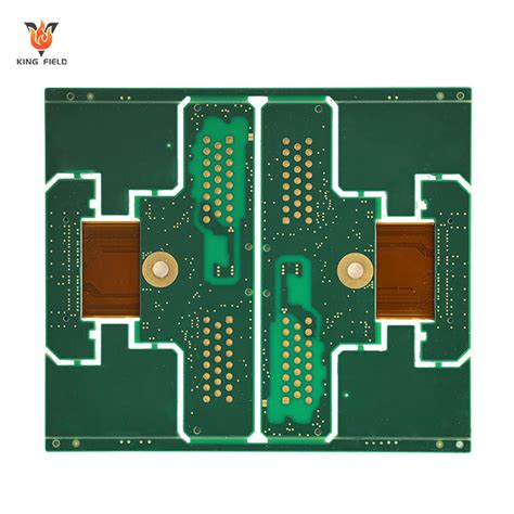
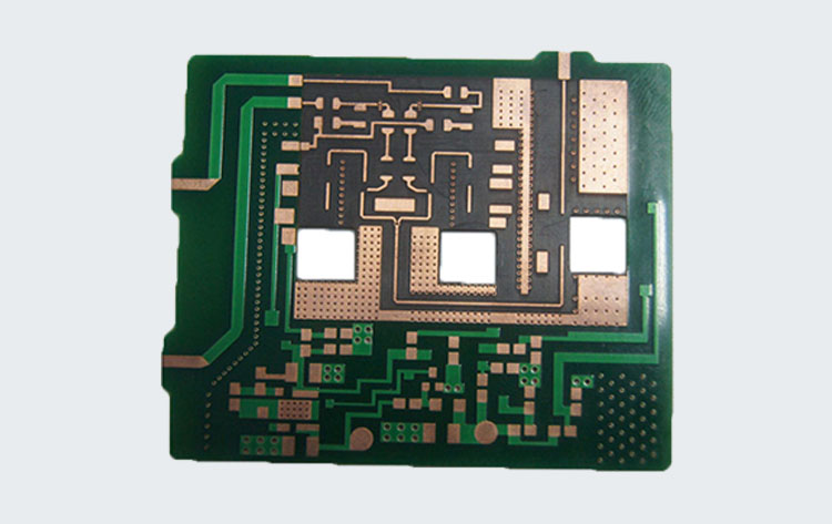
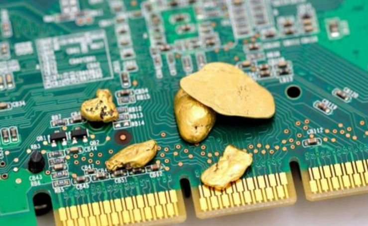
Chemical nickel-gold plating, namely ENIG (Electroless Nickel/Immersion Gold) process, is to chemically plate a layer of nickel on the surface of PCB copper foil, and then immerse it in a gold solution to deposit gold atoms on the nickel layer to form a thin and uniform gold layer.
2.Advantages of Chemical Nickel-Gold Plating Process
(1)Good solderability
The nickel-gold layer has excellent solderability, which can ensure a firm connection between electronic components and PCBs and improve welding quality and reliability. Whether in manual welding or automated welding, PCBs with chemical nickel-gold plating can show excellent welding performance.
(2)Excellent corrosion resistance
The nickel layer as the bottom layer can effectively prevent the oxidation and corrosion of the copper foil, while the gold layer further enhances the corrosion resistance of the PCB. Under harsh environmental conditions, the chemical nickel-gold-plated PCB can maintain long-term stability and reliability.
(3)Flat surface
The chemical nickel-gold plating process can form a very flat plating layer on the PCB surface, which is conducive to the installation and layout of electronic components. Especially for fine-pitch PCB design, the flat surface can improve the accuracy and reliability of welding.
(4)Good electrical performance
The nickel-gold layer has low contact resistance and good conductivity, which can ensure the stable transmission of electronic signals. At the same time, the chemical nickel-gold plating process can also reduce signal reflection and interference and improve the performance of electronic equipment.
3. Process of chemical nickel-gold plating process
(1)Pretreatment
Including cleaning, micro-etching, activation and other steps, the purpose is to remove oil, oxides and impurities on the PCB surface, so that the copper foil surface has good activity and prepare for the subsequent chemical nickel-gold plating.
(2)Chemical nickel plating
The PCB is immersed in a chemical plating solution containing nickel ions, and a nickel layer is deposited on the surface of the copper foil through a chemical reaction. The process of chemical nickel plating requires the control of parameters such as temperature, pH value, and plating solution concentration to ensure the quality and thickness of the nickel layer.
(3)Gold immersion
The surface of the PCB after chemical nickel plating is immersed in a gold solution to deposit gold atoms on the nickel layer to form a thin and uniform gold layer. The time and temperature of gold immersion also need to be strictly controlled to ensure the quality and thickness of the gold layer.
(4)Post-processing
Including steps such as cleaning and drying, the purpose is to remove residual plating solution and impurities on the surface of the PCB to make the PCB surface clean and tidy.
4. Challenges and solutions of chemical nickel plating process
(1)Black disk problem
During the process of chemical nickel plating, black disk phenomenon sometimes occurs, that is, a black area appears between the nickel layer and the gold layer, affecting the solderability and reliability of the PCB. The generation of the black disk problem is mainly related to factors such as the quality of the nickel layer, the thickness of the gold layer, the time and temperature of gold immersion. In order to solve the black disk problem, measures such as optimizing the process parameters of chemical nickel plating and immersion gold, improving the quality of pretreatment, and strengthening process control can be taken.
(2)Uneven gold layer thickness
Due to the complexity of the chemical nickel-gold plating process, the problem of uneven gold layer thickness sometimes occurs, affecting the appearance and performance of the PCB. In order to solve the problem of uneven gold layer thickness, measures such as optimizing the immersion gold process parameters, strengthening stirring and circulation, and improving the stability of the plating solution can be taken.
(3)High cost
The cost of the chemical nickel-gold plating process is relatively high, mainly due to the high price of the plating solution, the complex process, and the need for strict process control. In order to reduce costs, measures such as optimizing process parameters, improving production efficiency, and using low-cost raw materials can be taken.
5.Conclusion
As an important PCB surface treatment process, the chemical nickel-gold plating process has the advantages of good solderability, excellent corrosion resistance, flat surface and good electrical performance. However, the process also faces some challenges, such as black disk problems, uneven gold layer thickness and high cost. These problems can be effectively solved by optimizing process parameters, strengthening process control, and improving production efficiency, improving the quality and reliability of the chemical nickel-gold plating process, and providing strong support for the development of electronic equipment.