Diy pcb manufacturing
Essential Tools And Materials For DIY PCB Manufacturing
When embarking on the journey of DIY PCB (Printed Circuit Board) manufacturing, it is crucial to equip oneself with the essential tools and materials to ensure a successful and efficient process. The first step in this endeavor involves understanding the fundamental components required to create a functional PCB. This knowledge not only streamlines the manufacturing process but also enhances the quality and reliability of the final product.
To begin with, a high-quality PCB design software is indispensable.
Software such as Eagle, KiCad, or Altium Designer allows for precise schematic capture and layout design, which are critical for the accurate placement of components and routing of electrical connections. These tools provide a virtual environment to simulate and verify the circuit before physical manufacturing, thereby minimizing errors and optimizing performance.
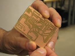
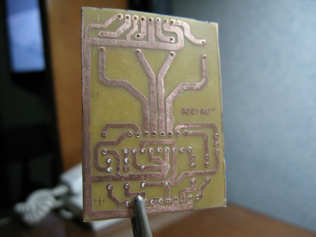
Once the design is finalized, the next essential material is the copper-clad board.
This board serves as the substrate for the PCB and is typically made of fiberglass or phenolic resin, coated with a thin layer of copper on one or both sides. The choice of single-sided or double-sided boards depends on the complexity of the circuit. For more intricate designs, double-sided boards offer additional routing options and flexibility.
In addition to the copper-clad board, a laser printer and glossy paper are necessary for the toner transfer method, a popular technique for transferring the PCB design onto the board. The design is printed onto the glossy paper using a laser printer, and then transferred to the copper-clad board using heat and pressure. An iron or a laminator can be employed to achieve this transfer, ensuring that the toner adheres firmly to the copper surface.
Following the toner transfer, an etching solution is required to remove the excess copper from the board, leaving only the desired circuit pattern. Ferric chloride is a commonly used etchant, although alternatives such as ammonium persulfate or cupric chloride are also available. It is important to handle these chemicals with care, using appropriate safety gear such as gloves and goggles, and to work in a well-ventilated area to avoid inhaling harmful fumes.
After etching, the next step involves drilling holes for through-hole components.
A precision drill press or a handheld rotary tool with fine drill bits is essential for this task. The diameter of the drill bits should match the size of the component leads to ensure a snug fit and reliable electrical connections.
To complete the PCB, soldering equipment is required. A temperature-controlled soldering iron, along with solder wire and flux, are fundamental tools for attaching components to the board. The soldering iron should have a fine tip for precision work, and the flux helps to clean the surfaces and improve the flow of solder, resulting in strong and conductive joints.
Finally, a multimeter is an invaluable tool for testing and troubleshooting the PCB.
It allows for the measurement of voltage, current, and resistance, helping to verify the integrity of the circuit and identify any potential issues.
In conclusion, DIY PCB manufacturing necessitates a comprehensive set of tools and materials, each playing a pivotal role in the creation of a functional and reliable circuit board. From design software and copper-clad boards to etching solutions and soldering equipment, every component is essential for achieving a successful outcome. By understanding and acquiring these tools, hobbyists and professionals alike can embark on their PCB manufacturing projects with confidence and precision..
Step-By-Step Guide To Designing Your Own PCB
Designing your own printed circuit board (PCB) can be a rewarding and cost-effective way to bring your electronic projects to life. The process, while intricate, is manageable with careful planning and attention to detail. This guide will walk you through the essential steps to create a functional and reliable PCB, from initial concept to final production.
To begin with, the first step in designing a PCB is to conceptualize your circuit.
This involves defining the purpose of your board and outlining the components required. It is crucial to have a clear understanding of the circuit’s functionality and the specifications of each component. Once you have a solid concept, you can proceed to create a schematic diagram. This diagram serves as a blueprint for your PCB, illustrating how each component connects within the circuit. Software tools such as Eagle, KiCad, or Altium Designer are commonly used for this purpose, offering a range of features to streamline the design process.
After completing the schematic, the next step is to design the PCB layout.
This involves translating the schematic into a physical representation of the board. During this phase, you will place components on the board and route the electrical connections between them. It is essential to consider factors such as component placement, trace width, and signal integrity. Proper component placement can significantly impact the board’s performance and manufacturability. For instance, placing components too close together can lead to soldering issues, while improper trace routing can cause signal interference.
Once the layout is finalized, the design must be checked for errors.
This is typically done through a process called Design Rule Checking (DRC), which ensures that the layout adheres to the manufacturing constraints and electrical rules. DRC tools can identify issues such as overlapping traces, insufficient spacing, and incorrect pad sizes. Addressing these errors early in the design process can save time and resources during manufacturing.
Following the DRC, the next step is to generate the Gerber files.
These files are the standard format used by PCB manufacturers to produce the board. Gerber files contain information about the copper layers, solder mask, silkscreen, and drill holes. It is important to review these files carefully to ensure they accurately represent your design. Many PCB design software tools offer built-in Gerber viewers to facilitate this review process.
With the Gerber files ready, you can proceed to the manufacturing stage.
There are numerous PCB fabrication services available, ranging from local providers to international companies. When selecting a manufacturer, consider factors such as cost, turnaround time, and quality. It is advisable to request a prototype run before committing to a large production batch. This allows you to test the board and make any necessary adjustments before full-scale manufacturing.
Once the boards are fabricated, the final step is assembly.
This involves soldering the components onto the PCB. Depending on the complexity of your design, this can be done manually or through automated processes such as pick-and-place machines and reflow ovens. It is crucial to follow proper soldering techniques to ensure reliable connections and avoid damaging the components.
In conclusion, designing your own PCB requires a methodical approach and attention to detail. By following these steps—conceptualizing the circuit, creating a schematic, designing the layout, checking for errors, generating Gerber files, selecting a manufacturer, and assembling the board—you can successfully bring your electronic projects to fruition. With practice and experience, the process will become more intuitive, allowing you to tackle increasingly complex designs.
Common Mistakes To Avoid In DIY PCB Production
In the realm of DIY PCB manufacturing, enthusiasts and professionals alike often encounter a variety of challenges that can impede the successful creation of printed circuit boards. Understanding and avoiding common mistakes is crucial to ensuring the efficiency and functionality of your PCBs. One prevalent error is the improper handling of design software. Many individuals underestimate the importance of thoroughly learning the software tools used for PCB design. This oversight can lead to design flaws that are not immediately apparent but become problematic during the manufacturing process. Therefore, investing time in mastering your design software is essential to avoid such pitfalls.
Another frequent mistake is neglecting to double-check the design for errors before proceeding to the manufacturing stage.
This includes verifying the placement of components, ensuring correct trace routing, and confirming that there are no unintentional short circuits. Utilizing design rule checks (DRC) within your software can help identify potential issues early on. Additionally, it is advisable to perform a thorough review of the schematic and layout to catch any discrepancies that might have been overlooked.
Transitioning from design to the physical creation of the PCB, one must be cautious about the quality of materials used.
Opting for low-quality copper-clad boards or substandard etching chemicals can result in poor conductivity and unreliable performance. It is imperative to source high-quality materials to ensure the longevity and reliability of your PCBs. Furthermore, the etching process itself requires meticulous attention. Inadequate etching can leave behind excess copper, leading to short circuits, while over-etching can remove necessary copper traces, disrupting the circuit’s functionality.
Soldering is another critical step where many DIY enthusiasts falter.
Poor soldering techniques can cause weak joints, which may fail under mechanical stress or thermal cycling. It is essential to use the correct type of solder and flux, maintain an appropriate soldering temperature, and ensure that each joint is clean and well-formed. Practicing good soldering habits, such as avoiding cold joints and ensuring proper wetting of the solder to the components and pads, can significantly enhance the reliability of your PCB.
Moreover, inadequate testing and inspection of the finished PCB can lead to undetected faults that compromise the entire project. It is crucial to conduct thorough testing, including continuity checks and functional tests, to verify that the PCB operates as intended. Utilizing tools such as multimeters and oscilloscopes can aid in identifying and diagnosing issues that may not be visible to the naked eye.
Additionally, improper storage and handling of components and finished PCBs can introduce defects.
Components should be stored in anti-static bags to prevent electrostatic discharge (ESD) damage, and finished PCBs should be handled with care to avoid physical damage or contamination. Ensuring a clean and organized workspace can also mitigate the risk of introducing errors during the assembly process.
In conclusion, DIY PCB manufacturing is a rewarding endeavor that requires careful attention to detail at every stage. By avoiding common mistakes such as inadequate software proficiency, insufficient design verification, poor material quality, subpar soldering techniques, lack of thorough testing, and improper handling, one can significantly improve the chances of producing high-quality, reliable PCBs. Embracing a meticulous and informed approach will not only enhance the success of your projects but also contribute to the development of your skills and expertise in the field of PCB manufacturing.
Advanced Techniques For High-Quality DIY PCBs
Creating high-quality DIY printed circuit boards (PCBs) requires a blend of precision, patience, and advanced techniques. As hobbyists and professionals alike seek to produce reliable and efficient PCBs, understanding the nuances of advanced manufacturing methods becomes essential. One of the first steps in achieving superior results is mastering the art of designing the PCB layout. Utilizing sophisticated software such as KiCad or Eagle can significantly enhance the accuracy of your design. These tools offer extensive libraries of components and advanced features like auto-routing, which can streamline the design process and minimize errors.
Once the design is finalized, the next critical phase involves transferring the design onto the PCB substrate.
Traditional methods like the toner transfer technique have been widely used, but for higher quality, the photoresist method is often preferred. This technique involves printing the PCB layout onto a transparent film, which is then used to expose a photoresist-coated PCB to ultraviolet light. The exposed areas harden, while the unexposed areas remain soluble and can be washed away, leaving a precise pattern of the circuit.
Etching is another pivotal step where precision is paramount.
Ferric chloride is a common etchant, but for those seeking cleaner and more controlled results, cupric chloride or ammonium persulfate can be used. These chemicals offer a more consistent etching process, reducing the risk of undercutting and ensuring finer details are preserved. It is crucial to monitor the etching process closely and agitate the solution gently to achieve uniform results.
Drilling the PCB holes accurately is another aspect that can significantly impact the quality of the final product.
Using a high-speed rotary tool with carbide drill bits can provide the precision needed for small and densely packed components. Additionally, employing a drill press or a CNC machine can further enhance accuracy and reduce the risk of misalignment.
Soldering is the final step in assembling the PCB, and it requires a steady hand and attention to detail. Using a high-quality soldering iron with adjustable temperature control can prevent damage to sensitive components. Moreover, opting for lead-free solder, while environmentally friendly, requires a slightly higher temperature and more precise control to ensure strong and reliable joints. Flux is also an indispensable aid in the soldering process, as it helps to clean the surfaces and improve the flow of solder, resulting in better connections.
To further elevate the quality of your DIY PCBs, consider implementing surface-mount technology (SMT).
SMT allows for smaller and more compact designs, which can be particularly beneficial for modern electronic devices. While it requires specialized equipment such as a reflow oven or a hot air rework station, the investment can be worthwhile for those regularly producing high-quality PCBs.
Testing and quality control are the final, yet crucial, stages in the manufacturing process. Using a multimeter to check for continuity and shorts can help identify any issues before the PCB is put into operation. Additionally, employing an oscilloscope can provide insights into the performance of the circuit under real-world conditions, ensuring that it meets the desired specifications.
In conclusion, achieving high-quality DIY PCBs involves a combination of advanced techniques and meticulous attention to detail. From precise design and accurate transfer methods to careful etching, drilling, and soldering, each step plays a vital role in the overall success of the project. By embracing these advanced techniques, hobbyists and professionals alike can produce PCBs that rival commercially manufactured counterparts, paving the way for innovative and reliable electronic solutions.


