Don’t get confused anymore! Teach you to distinguish through holes, blind holes, and buried holes in PCBs!
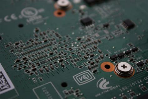
In the field of electronic manufacturing, PCBs are important carriers for electrical connections of electronic components. In the design and manufacturing process of PCBs, through holes, blind holes, and buried holes are three common types of holes, which play a vital role in the electrical connection, structural support, and signal transmission of circuit boards.
This article will elaborate on the definition, characteristics, and application scenarios of these three holes to help you better understand and distinguish them.
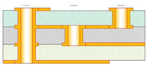
1.Through Hole (PTH)
Definition: A through hole is a hole that passes from one side of a circuit board to the other side and can completely penetrate the entire circuit board. They are usually used to connect circuits at different levels to provide electrical connections and mechanical support.
Features:
Structure: Through holes have a larger diameter and depth to accommodate the size and insertion depth of component pins.
Manufacturing process: Through holes are usually made using mechanical drills or laser drilling technology, and metallization is performed after drilling to form a conductive layer to achieve electrical connection.
Application: Through holes are suitable for components that require mechanical support and electrical connections, such as traditional plug-in components (resistors, capacitors, inductors, etc.). In high-density interconnect (HDI) PCBs, through holes can also be used to achieve electrical connections between multilayer boards.
Advantages and Disadvantages: Through holes are relatively cheap to make and easy to make, but they may occupy more PCB board area and limit the density of circuit layout. In addition, through holes themselves have certain inductance and capacitance characteristics, which may have a negative impact on signal transmission in high-frequency and high-speed circuits.
2.Blind Via Hole (BVH)
Definition: Blind vias are holes that enter the circuit board only from one side and do not penetrate the entire board thickness. They are mainly used to connect circuits between surface layers and internal layers.
Features:
Structure: Blind holes are usually smaller in size to accommodate the tight layout in multilayer boards. They are only visible from one side of the circuit board and do not penetrate the entire board thickness.
Manufacturing process: Blind holes are mainly made using laser drilling technology, which is characterized by high precision and high efficiency. In some cases, chemical etching technology can also be used, but this method is usually used to make larger holes with lower precision. Blind vias also require metallization to achieve electrical connections.
Application: Blind vias are widely used in multi-layer PCBs, especially high-density interconnect (HDI) PCBs that require electrical connections between internal layers. In the fields of wireless communications, mobile devices, consumer electronics, etc., the use of blind vias can significantly improve the integration and signal transmission efficiency of circuit boards.
Advantages and disadvantages: Blind vias can increase the density of circuit layout and reduce the impact of external surfaces, but the production cost and difficulty are high, and the drilling depth needs to be precisely controlled to avoid electroplating difficulties.
3.Buried Via Hole (BVH)
Definition: Buried vias are holes that are completely located inside the circuit board, neither entering or exiting from one side nor penetrating the entire board thickness. They are used to connect circuits between internal layers without affecting the external surface.
Features:
Structure: Buried vias are completely located inside the circuit board and cannot be directly observed from the outside. They achieve electrical connection through metallized inner walls and are usually used for hidden connections in multi-layer boards.
Manufacturing process: The manufacturing process of buried vias is relatively complicated, including local drilling and then electroplating. Since the operation process is more complicated than through holes and blind holes, the price is relatively more expensive.
Application: Buried holes are mainly used for hidden connections in multi-layer PCBs, especially in situations where the surface flatness of the circuit board needs to be maintained. In the fields of high-performance computing, military electronics, aerospace, etc., the use of buried holes can significantly improve the reliability and stability of circuit boards.
Advantages and disadvantages: Buried holes can improve space utilization and signal transmission quality, reduce signal delay and cross interference, but the production process is complicated and the cost is high.
The application of through holes, blind holes and buried holes in PCBs has different focuses. Through holes are suitable for simple connections and cost-sensitive applications. Their structure is obvious and runs through the entire circuit board; blind holes are suitable for multi-layer board designs with limited space. They only enter the circuit board from one side and do not penetrate the entire board thickness; while buried holes play an important role in circuit boards that pursue high density and high performance. They are completely inside the circuit board and cannot be directly observed from the outside.
In practical applications, it is necessary to select the appropriate hole type according to the needs and performance requirements of the circuit design. For example, in components that require mechanical support and electrical connections, through holes are the first choice; in multi-layer boards, where electrical connections between internal layers are required and space requirements are high, blind and buried vias are more advantageous.