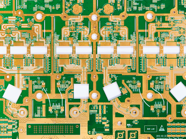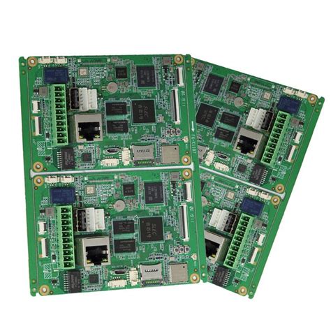
Double sided flexible pcb
Advantages Of Double Sided Flexible PCBs In Modern Electronics
Double-sided flexible printed circuit boards (PCBs) have emerged as a pivotal component in the realm of modern electronics, offering a multitude of advantages that cater to the ever-evolving demands of contemporary technology. As electronic devices continue to shrink in size while expanding in functionality, the need for innovative solutions like double-sided flexible PCBs becomes increasingly apparent. These advanced circuit boards provide a unique combination of flexibility, durability, and efficiency, making them indispensable in a wide array of applications.
One of the primary advantages of double-sided flexible PCBs is their ability to accommodate complex circuit designs within a compact form factor.
Unlike traditional rigid PCBs, which are limited by their inflexible nature, double-sided flexible PCBs can be bent, folded, and twisted to fit into tight spaces. This flexibility is particularly beneficial in the design of wearable technology, medical devices, and compact consumer electronics, where space is at a premium. By allowing circuits to be placed on both sides of the substrate, these PCBs effectively double the available surface area for components, enabling more intricate and sophisticated designs without increasing the overall size of the device.
In addition to their space-saving capabilities, double-sided flexible PCBs also offer enhanced reliability and performance.
The use of flexible materials such as polyimide or polyester not only provides the necessary pliability but also contributes to the board’s resilience against mechanical stress and environmental factors. This durability is crucial in applications where the circuit board may be subjected to frequent movement or harsh conditions, such as in automotive or aerospace industries. Furthermore, the ability to incorporate plated through-holes in double-sided designs ensures robust electrical connections between the two layers, reducing the risk of circuit failure and enhancing the overall reliability of the device.
Another significant advantage of double-sided flexible PCBs is their potential for cost savings in both manufacturing and assembly processes.
The reduction in the number of interconnects and connectors required, due to the ability to integrate more components on a single board, leads to a decrease in material costs and assembly time. Moreover, the lightweight nature of flexible PCBs contributes to lower shipping costs and easier handling during production. These economic benefits make double-sided flexible PCBs an attractive option for manufacturers looking to optimize their production processes while maintaining high-quality standards.
The versatility of double-sided flexible PCBs extends beyond their physical attributes, as they also offer significant design flexibility.
Engineers can leverage the dual-layer configuration to implement more complex circuit architectures, such as incorporating additional functionalities or improving signal integrity. This adaptability is particularly advantageous in the development of cutting-edge technologies, where rapid prototyping and iterative design processes are essential. By facilitating quick modifications and adjustments, double-sided flexible PCBs enable faster time-to-market for new products, providing a competitive edge in the fast-paced electronics industry.
In conclusion, the advantages of double-sided flexible PCBs in modern electronics are manifold, encompassing space efficiency, enhanced reliability, cost-effectiveness, and design versatility. As the demand for smaller, more powerful, and more reliable electronic devices continues to grow, the role of double-sided flexible PCBs is set to become even more prominent. By addressing the challenges posed by traditional circuit board technologies, these innovative solutions are paving the way for the next generation of electronic devices, driving progress and innovation across various sectors.
Design Considerations For Double Sided Flexible PCBs
When designing double-sided flexible printed circuit boards (PCBs), several critical considerations must be taken into account to ensure optimal performance and reliability. These PCBs, known for their adaptability and space-saving capabilities, are increasingly utilized in various applications, from consumer electronics to medical devices.
To begin with, understanding the material selection is paramount.
Flexible PCBs are typically made from polyimide or polyester films, which offer excellent flexibility and thermal stability. The choice of material impacts not only the mechanical properties but also the electrical performance of the circuit. Therefore, designers must carefully evaluate the material’s dielectric constant, thermal expansion coefficient, and moisture absorption characteristics to match the application’s specific requirements.
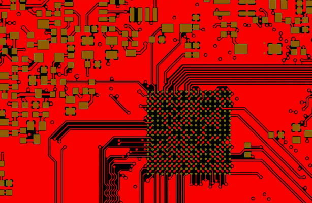
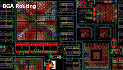
Transitioning to the layout design, it is essential to consider the trace routing on both sides of the PCB.
Double-sided flexible PCBs allow for more complex circuit designs by providing additional routing space. However, this complexity necessitates meticulous planning to avoid issues such as crosstalk and signal interference. Designers should employ techniques like controlled impedance and differential pair routing to maintain signal integrity. Additionally, the use of vias, which connect traces on different layers, should be minimized to preserve the board’s flexibility and reduce potential stress points.
Moreover, the bending and folding requirements of the application must be factored into the design process.
Flexible PCBs are often subjected to dynamic mechanical stresses, and improper design can lead to failure. To mitigate this risk, designers should incorporate bend radius guidelines and avoid placing components or vias in areas subject to frequent bending. Furthermore, the use of strain relief features, such as curved traces and filleted corners, can enhance the board’s durability under mechanical stress.
In addition to mechanical considerations, thermal management is another critical aspect of double-sided flexible PCB design.
These boards are often used in compact devices where heat dissipation is a concern. Effective thermal management strategies, such as the use of thermal vias and heat spreaders, can help dissipate heat away from critical components. Additionally, selecting materials with high thermal conductivity can further enhance the board’s ability to manage heat.
Transitioning to the manufacturing process, it is crucial to collaborate closely with PCB manufacturers during the design phase.
Double-sided flexible PCBs require specialized fabrication techniques, and early communication with manufacturers can help identify potential challenges and optimize the design for manufacturability. This collaboration can also aid in selecting appropriate surface finishes and solder mask options that align with the application’s environmental and operational conditions.
Finally, testing and validation are indispensable steps in the design process.
Rigorous testing, including electrical, mechanical, and environmental assessments, ensures that the PCB meets the desired performance criteria. Designers should also consider implementing design for testability (DFT) features, such as test points and access pads, to facilitate efficient testing and troubleshooting.
In conclusion, designing double-sided flexible PCBs involves a comprehensive understanding of material properties, layout strategies, mechanical and thermal considerations, and manufacturing processes. By addressing these factors with meticulous attention to detail, designers can create robust and reliable flexible PCBs that meet the demands of modern electronic applications. Through careful planning and collaboration, the potential of double-sided flexible PCBs can be fully realized, paving the way for innovative and compact electronic solutions.
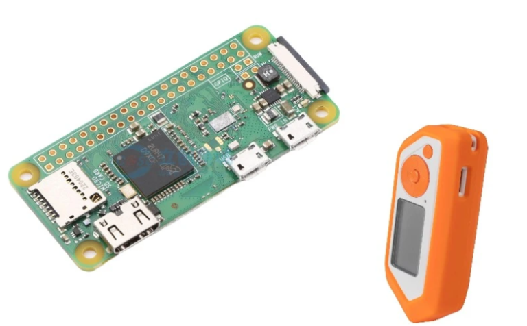
Applications Of Double Sided Flexible PCBs In Wearable Technology
Double-sided flexible printed circuit boards (PCBs) have emerged as a pivotal component in the rapidly evolving field of wearable technology. These innovative circuit boards offer a unique combination of flexibility, durability, and compactness, making them ideally suited for the demands of wearable devices. As the wearable technology market continues to expand, driven by consumer demand for more integrated and multifunctional devices, the applications of double-sided flexible PCBs are becoming increasingly diverse and sophisticated.
One of the primary applications of double-sided flexible PCBs in wearable technology is in the development of smartwatches.
These devices require a compact and efficient design to house various components such as sensors, processors, and communication modules. Double-sided flexible PCBs provide the necessary space-saving benefits by allowing components to be mounted on both sides of the board. This capability not only reduces the overall size of the device but also enhances its functionality by accommodating more features within a limited space. Furthermore, the flexibility of these PCBs allows them to conform to the curved surfaces of smartwatch designs, ensuring a seamless integration that enhances both aesthetics and user comfort.
In addition to smartwatches, fitness trackers also benefit significantly from the use of double-sided flexible PCBs.
These devices are designed to be lightweight and comfortable for continuous wear, often during physical activities. The flexibility of the PCBs ensures that the devices can withstand the constant movement and bending that occurs during exercise, without compromising their performance or durability. Moreover, the ability to mount components on both sides of the PCB allows for the inclusion of advanced features such as heart rate monitors, GPS modules, and wireless connectivity, all within a compact form factor.
Beyond consumer electronics, double-sided flexible PCBs are also finding applications in the medical sector, particularly in wearable health monitoring devices.
These devices, which include patches and bands that monitor vital signs, require a high degree of reliability and precision. The dual-sided nature of these PCBs allows for the integration of multiple sensors and data processing units, enabling continuous and accurate monitoring of health parameters. Additionally, the flexibility of the PCBs ensures that the devices can be comfortably worn on various parts of the body, providing patients with a non-intrusive means of health monitoring.
Furthermore, the integration of double-sided flexible PCBs in wearable technology extends to the realm of augmented reality (AR) and virtual reality (VR) headsets.
These devices demand a high level of performance and connectivity, which can be achieved through the use of advanced PCBs. The dual-sided design facilitates the incorporation of high-speed processors, memory units, and communication interfaces, all while maintaining a lightweight and ergonomic design. This is crucial for ensuring user comfort during extended periods of use, as well as for delivering an immersive AR or VR experience.
In conclusion, the applications of double-sided flexible PCBs in wearable technology are vast and varied, driven by the need for compact, reliable, and multifunctional devices. From consumer electronics like smartwatches and fitness trackers to medical monitoring devices and AR/VR headsets, these PCBs play a critical role in advancing the capabilities and performance of wearable technology. As the industry continues to innovate, the demand for such versatile and efficient circuit solutions is expected to grow, further cementing the importance of double-sided flexible PCBs in the future of wearable technology.

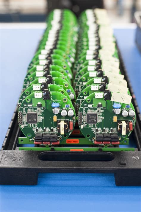
Manufacturing Process Of Double Sided Flexible PCBs
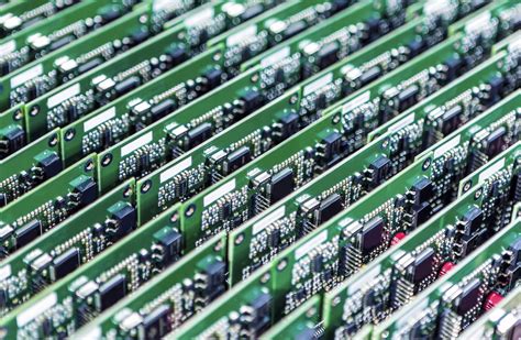
The manufacturing process of double-sided flexible printed circuit boards (PCBs) is a sophisticated and intricate procedure that requires precision and expertise. These PCBs are essential in modern electronics due to their ability to fit into compact spaces while maintaining high functionality.
The process begins with the selection of appropriate materials, which is crucial for ensuring the flexibility and durability of the final product. Typically, a polyimide film is used as the substrate due to its excellent thermal stability and mechanical properties. This substrate is then coated with a thin layer of copper on both sides, which serves as the conductive material.
Once the substrate is prepared, the next step involves the application of a photoresist layer.
This is a light-sensitive material that is applied to both sides of the copper-clad substrate. The photoresist is then exposed to ultraviolet light through a photomask, which contains the desired circuit pattern. The areas of the photoresist exposed to the light become hardened, while the unexposed areas remain soft. This differential exposure allows for the subsequent development process, where the soft areas of the photoresist are washed away, revealing the underlying copper.
Following the development of the photoresist, the exposed copper areas are etched away using a chemical solution, typically ferric chloride or ammonium persulfate.
This etching process removes the unwanted copper, leaving behind the desired circuit pattern on both sides of the substrate. It is crucial to control the etching process precisely to ensure that the copper traces are of the correct width and spacing, as any deviation can affect the performance of the PCB.
After etching, the remaining photoresist is stripped away, revealing the clean copper traces.
At this stage, the double-sided flexible PCB begins to take shape, but further processing is required to enhance its functionality and reliability. One such process is the application of a protective solder mask, which is applied over the copper traces to prevent oxidation and short circuits. The solder mask also provides a surface for soldering components onto the PCB.
To facilitate the connection of components, vias are drilled through the PCB.
These are small holes that allow electrical connections between the two sides of the board. The vias are then plated with copper to ensure conductivity. This step is critical for double-sided PCBs, as it enables the integration of more complex circuits within a limited space.
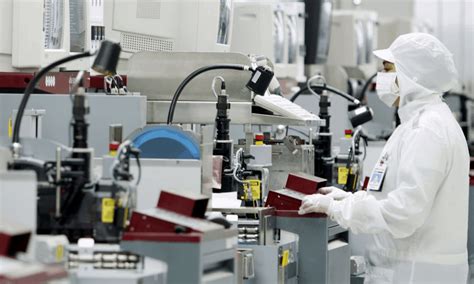
Finally, the PCB undergoes a series of tests to ensure its functionality and reliability.
These tests include electrical testing to verify the continuity and isolation of the circuits, as well as mechanical testing to assess the flexibility and durability of the board. Any defects identified during testing are addressed before the PCB is approved for use.
In conclusion, the manufacturing process of double-sided flexible PCBs is a meticulous and multi-step procedure that combines material science, photolithography, and chemical processing. Each step is carefully controlled to produce a high-quality product that meets the demanding requirements of modern electronic devices. As technology continues to advance, the demand for flexible PCBs is expected to grow, driving further innovations in their manufacturing processes.