Double-Sided PCB Assembly: A Comprehensive Guide
Introduction
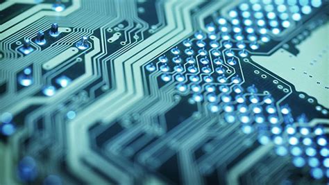
Printed Circuit Boards (PCBs) are the backbone of modern electronics, providing the necessary platform for mounting and interconnecting electronic components. As technology advances, the demand for more complex and compact electronic devices has led to the widespread adoption of double-sided PCB assembly. Unlike single-sided PCBs, which have conductive traces on only one side, double-sided PCBs feature conductive layers on both sides of the board. This allows for higher component density and more complex circuit designs, making double-sided PCBs ideal for a wide range of applications, from consumer electronics to industrial machinery.
This article delves into the intricacies of double-sided PCB assembly, covering the design considerations, manufacturing processes, advantages, challenges, and applications of double-sided PCBs.
1. Design Considerations for Double-Sided PCBs
Designing a double-sided PCB requires careful planning to ensure optimal performance, manufacturability, and reliability. Key considerations include:
1.1. Component Placement
One of the primary advantages of double-sided PCBs is the ability to place components on both sides of the board. However, this also introduces complexity in terms of component placement and routing. Designers must consider factors such as thermal management, signal integrity, and mechanical stability when placing components on both sides of the board.
- Thermal Management: Components that generate significant heat should be placed on the top side of the board to facilitate heat dissipation. If heat-generating components are placed on the bottom side, additional thermal management techniques, such as heat sinks or thermal vias, may be required.
- Signal Integrity: High-speed signals should be routed on the inner layers of the board to minimize interference and crosstalk. If high-speed components are placed on both sides of the board, careful attention must be paid to signal routing and impedance matching.
- Mechanical Stability: Components that are subject to mechanical stress, such as connectors or large capacitors, should be placed on the top side of the board to ensure stability during assembly and operation.
1.2. Routing and Via Placement
Routing traces on a double-sided PCB requires careful planning to avoid signal interference and ensure reliable connections between components. Vias, which are used to connect traces on different layers, play a crucial role in double-sided PCB design.
- Via Types: There are several types of vias, including through-hole vias, blind vias, and buried vias. Through-hole vias are the most common and are used to connect traces on both sides of the board. Blind vias connect an outer layer to an inner layer, while buried vias connect inner layers without reaching the outer layers.
- Via Placement: Vias should be placed strategically to minimize signal interference and ensure reliable connections. High-speed signals should be routed with minimal via usage to reduce signal degradation. Additionally, vias should be placed away from high-voltage or high-current traces to prevent electrical interference.
1.3. Layer Stackup
The layer stackup of a double-sided PCB refers to the arrangement of conductive and insulating layers within the board. While double-sided PCBs have only two conductive layers, the choice of materials and thicknesses can significantly impact the board’s performance.
- Dielectric Material: The dielectric material between the conductive layers affects the board’s electrical properties, such as impedance and signal propagation speed. Common dielectric materials include FR-4, polyimide, and Rogers materials, each with its own set of properties and applications.
- Copper Thickness: The thickness of the copper layers affects the board’s current-carrying capacity and thermal performance. Thicker copper layers are used for high-current applications, while thinner layers are suitable for low-power circuits.
2. Manufacturing Processes for Double-Sided PCB Assembly
The manufacturing process for double-sided PCB assembly involves several steps, each of which must be carefully executed to ensure the quality and reliability of the final product.
2.1. PCB Fabrication
The first step in double-sided PCB assembly is the fabrication of the bare PCB. This process involves the following steps:
- Substrate Preparation: The base material, typically a fiberglass-reinforced epoxy laminate (FR-4), is cut to the desired size and shape. The substrate is then cleaned to remove any contaminants that could affect the adhesion of the conductive layers.
- Copper Cladding: A thin layer of copper is laminated onto both sides of the substrate. The thickness of the copper layer depends on the design requirements and the intended application of the PCB.
- Drilling: Holes are drilled through the substrate to create vias and mounting holes for through-hole components. The drilling process must be precise to ensure proper alignment and connectivity between layers.
- Plating: The drilled holes are plated with copper to create electrical connections between the layers. This process, known as through-hole plating, ensures that the vias are conductive and reliable.
- Etching: A photoresist layer is applied to the copper-clad substrate, and a photomask is used to expose the desired circuit pattern. The exposed copper is then etched away, leaving behind the conductive traces.
- Solder Mask Application: A solder mask is applied to both sides of the board to protect the copper traces from oxidation and prevent solder bridges during assembly. The solder mask also provides electrical insulation between adjacent traces.
- Silkscreen Printing: Component labels, logos, and other markings are printed onto the board using a silkscreen process. This step helps with component placement and identification during assembly.
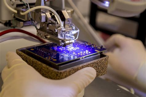
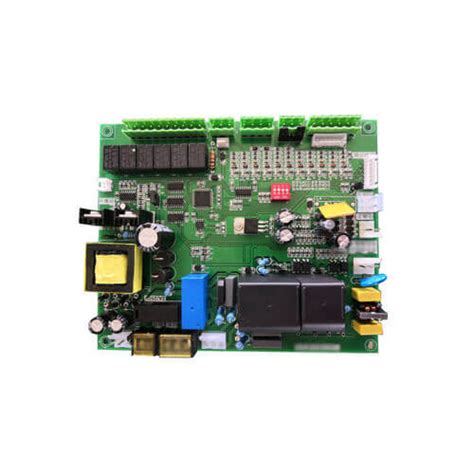
2.2. Component Placement
Once the bare PCB is fabricated, the next step is to place the electronic components onto the board. This process can be done manually or using automated pick-and-place machines, depending on the complexity and volume of the assembly.
- Surface Mount Technology (SMT): SMT components are placed directly onto the surface of the PCB and soldered in place. SMT components are smaller and lighter than through-hole components, making them ideal for high-density designs.
- Through-Hole Technology (THT): THT components are inserted into pre-drilled holes on the PCB and soldered on the opposite side. THT components are typically used for high-power or high-reliability applications where mechanical stability is critical.
2.3. Soldering
Soldering is the process of joining the components to the PCB using a molten metal alloy. There are several soldering techniques used in double-sided PCB assembly:
- Reflow Soldering: Reflow soldering is the most common method for soldering SMT components. The PCB is passed through a reflow oven, where the solder paste is heated to its melting point, forming a permanent bond between the components and the board.
- Wave Soldering: Wave soldering is typically used for THT components. The PCB is passed over a wave of molten solder, which wets the exposed metal surfaces and forms a solder joint.
- Selective Soldering: Selective soldering is used for mixed-technology boards that contain both SMT and THT components. A robotic soldering head is used to apply solder only to the THT components, avoiding the SMT components.
2.4. Inspection and Testing
After soldering, the assembled PCB undergoes a series of inspections and tests to ensure quality and functionality.
- Visual Inspection: The board is visually inspected for defects such as solder bridges, misaligned components, or damaged traces. Automated optical inspection (AOI) systems are often used to detect defects that may be missed by the human eye.
- X-Ray Inspection: X-ray inspection is used to examine hidden solder joints, such as those under BGA (Ball Grid Array) components. This technique is particularly useful for detecting voids or insufficient solder in hidden joints.
- Electrical Testing: Electrical testing, such as in-circuit testing (ICT) or functional testing, is performed to verify the electrical performance of the board. ICT checks for shorts, opens, and component values, while functional testing verifies that the board operates as intended.
3. Advantages of Double-Sided PCB Assembly
Double-sided PCB assembly offers several advantages over single-sided PCBs, making it a popular choice for a wide range of applications.
3.1. Increased Component Density
By utilizing both sides of the board, double-sided PCBs can accommodate a higher number of components, allowing for more complex and compact designs. This is particularly important in modern electronics, where space is often at a premium.
3.2. Improved Signal Routing
Double-sided PCBs provide more routing options, allowing designers to optimize signal paths and reduce the length of high-speed traces. This can improve signal integrity and reduce electromagnetic interference (EMI).
3.3. Enhanced Thermal Management
With components on both sides of the board, double-sided PCBs offer better thermal management options. Heat-generating components can be placed on the top side for better heat dissipation, while additional thermal vias can be used to transfer heat to the bottom side.
3.4. Cost-Effectiveness
While double-sided PCBs are more complex to design and manufacture than single-sided PCBs, they are often more cost-effective for high-density designs. By reducing the overall size of the board, double-sided PCBs can lower material and assembly costs.
4. Challenges in Double-Sided PCB Assembly
Despite their advantages, double-sided PCBs present several challenges that must be addressed during design and manufacturing.
4.1. Complex Design and Routing
Designing a double-sided PCB requires careful planning and attention to detail. The increased complexity of routing traces on both sides of the board can lead to signal integrity issues, crosstalk, and EMI if not properly managed.
4.2. Soldering Difficulties
Soldering components on both sides of the board can be challenging, particularly for through-hole components. Specialized soldering techniques, such as selective soldering, may be required to ensure reliable solder joints.
4.3. Inspection and Testing
Inspecting and testing double-sided PCBs can be more complex than single-sided PCBs, particularly for hidden solder joints. Advanced inspection techniques, such as X-ray inspection, may be required to ensure the quality of the assembly.
5. Applications of Double-Sided PCBs
Double-sided PCBs are used in a wide range of applications, from consumer electronics to industrial machinery. Some common applications include:
5.1. Consumer Electronics
Double-sided PCBs are widely used in consumer electronics, such as smartphones, tablets, and laptops. The high component density and compact design of double-sided PCBs make them ideal for these applications.
5.2. Automotive Electronics
The automotive industry relies on double-sided PCBs for various electronic systems, including engine control units (ECUs), infotainment systems, and advanced driver-assistance systems (ADAS). The robust design and thermal management capabilities of double-sided PCBs make them suitable for the harsh environments found in automotive applications.
5.3. Industrial Machinery
Double-sided PCBs are used in industrial machinery for control systems, power supplies, and communication modules. The ability to handle high currents and temperatures makes double-sided PCBs ideal for these demanding applications.
5.4. Medical Devices
Medical devices, such as imaging equipment, patient monitors, and diagnostic tools, often use double-sided PCBs. The high reliability and compact design of double-sided PCBs are critical for these life-saving applications.
Conclusion
Double-sided PCB assembly is a critical technology in modern electronics, enabling the development of complex, high-density, and compact electronic devices. While the design and manufacturing processes for double-sided PCBs are more complex than those for single-sided PCBs, the benefits in terms of component density, signal routing, thermal management, and cost-effectiveness make them an attractive choice for a wide range of applications.
As technology continues to advance, the demand for double-sided PCBs is expected to grow, driving further innovation in PCB design and manufacturing techniques. By understanding the intricacies of double-sided PCB assembly, designers and manufacturers can create high-quality, reliable electronic products that meet the ever-increasing demands of the modern world.


