Double-Sided PCB Assembly: Techniques, Advantages, and Applications
Introduction
Double-sided PCB assembly is a widely used manufacturing process in the electronics industry, offering a balance between complexity and cost-effectiveness. Unlike single-sided PCBs, which have components and traces on only one side, double-sided PCBs utilize both sides of the board, allowing for higher component density and more complex circuit designs. This article explores the techniques, advantages, challenges, and applications of double-sided PCB assembly, providing a comprehensive understanding of this critical process.
1. What is Double-Sided PCB Assembly?
1.1 Definition
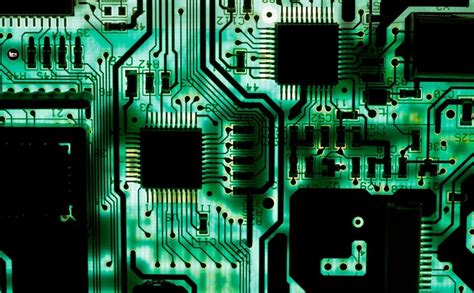
Double-sided PCB assembly involves mounting electronic components and routing conductive traces on both sides of a printed circuit board. This approach increases the available space for components and interconnections, making it ideal for more complex and compact designs.
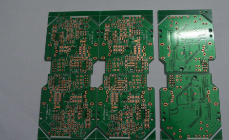
1.2 Structure of a Double-Sided PCB
A double-sided PCB consists of:
- Substrate: A non-conductive base material, typically made of fiberglass (FR-4).
- Copper Layers: Conductive layers on both sides of the substrate.
- Solder Mask: A protective layer that prevents solder bridges and short circuits.
- Silkscreen: Labels and markings for component placement and identification.
- Vias: Plated-through holes that connect traces on both sides of the board.
2. Advantages of Double-Sided PCB Assembly
2.1 Increased Component Density
Double-sided PCBs allow for more components to be placed on a single board, making them suitable for compact and high-performance devices.
2.2 Enhanced Design Flexibility
Designers can route traces on both sides of the board, enabling more complex and efficient circuit layouts.
2.3 Cost-Effective for Mid-Complexity Designs
Double-sided PCBs strike a balance between the simplicity of single-sided boards and the complexity of multi-layer boards, making them cost-effective for many applications.
2.4 Improved Signal Integrity
Shorter trace lengths and optimized routing reduce signal interference and improve electrical performance.
2.5 Versatility
Double-sided PCBs are used in a wide range of applications, from consumer electronics to industrial equipment.
3. Double-Sided PCB Assembly Process
The assembly process for double-sided PCBs involves several steps, each requiring precision and attention to detail.
3.1 Design and Layout
The process begins with the design of the PCB using CAD software. Key considerations include:
- Component Placement: Optimizing the layout to minimize trace lengths and avoid interference.
- Via Placement: Strategically placing vias to connect traces on both sides.
- Thermal Management: Ensuring proper heat dissipation for high-power components.
3.2 PCB Fabrication
The fabrication process includes:
- Substrate Preparation: Cutting and cleaning the base material.
- Copper Lamination: Applying copper layers to both sides of the substrate.
- Etching: Removing unwanted copper to create the desired traces.
- Drilling: Creating holes for vias and through-hole components.
- Plating: Electrically connecting the layers through plated-through holes.
- Solder Mask and Silkscreen Application: Adding protective and labeling layers.
3.3 Component Placement
Components are placed on both sides of the PCB using automated pick-and-place machines. The process involves:
- Solder Paste Application: Applying solder paste to the pads using a stencil.
- Component Placement: Positioning components on the solder paste with high precision.
3.4 Reflow Soldering
The PCB is passed through a reflow oven, where the solder paste melts and forms solid solder joints. For double-sided PCBs, this process is typically done in two stages:
- First Side Reflow: Soldering components on the first side.
- Second Side Reflow: Soldering components on the second side, often using a lower temperature to avoid re-melting the first side’s solder joints.
3.5 Through-Hole Component Assembly
If the design includes through-hole components, they are inserted and soldered after the reflow process. This can be done using wave soldering or manual soldering.
3.6 Testing and Inspection
After assembly, the PCB undergoes rigorous testing and inspection to ensure functionality and quality. Common methods include:
- Automated Optical Inspection (AOI): Detecting visual defects such as misaligned components or solder bridges.
- In-Circuit Testing (ICT): Verifying the electrical performance of individual components.
- Functional Testing: Ensuring the assembled PCB performs its intended function.
4. Challenges in Double-Sided PCB Assembly
4.1 Thermal Management
Soldering components on both sides requires careful thermal management to avoid damaging components or re-melting solder joints.
4.2 Component Placement
Accurate placement of components on both sides is critical to avoid interference and ensure proper functionality.
4.3 Via Reliability
Vias must be properly designed and manufactured to ensure reliable electrical connections between layers.
4.4 Testing Complexity
Testing double-sided PCBs can be more complex due to the increased number of components and connections.
5. Applications of Double-Sided PCB Assembly
Double-sided PCBs are used in a wide range of industries and applications, including:
5.1 Consumer Electronics
- Smartphones and Tablets: High component density and compact designs.
- Wearable Devices: Lightweight and flexible layouts.
5.2 Automotive
- Engine Control Units (ECUs): Reliable performance in harsh environments.
- Infotainment Systems: Complex circuits for audio and video processing.
5.3 Industrial Equipment
- Control Systems: Robust designs for industrial automation.
- Power Supplies: Efficient power management and distribution.
5.4 Medical Devices
- Diagnostic Equipment: High precision and reliability.
- Wearable Health Monitors: Compact and lightweight designs.
5.5 Aerospace and Defense
- Avionics: High-performance circuits for navigation and communication.
- Military Equipment: Durable and reliable designs for harsh conditions.
6. Future Trends in Double-Sided PCB Assembly
6.1 Advanced Materials
New materials, such as high-temperature substrates and flexible polymers, are expanding the possibilities for double-sided PCB designs.
6.2 Miniaturization
As electronic devices become smaller, double-sided PCBs are being designed with even higher component densities and finer trace widths.
6.3 Automation and Industry 4.0
The integration of automation, IoT, and AI is improving the efficiency and precision of double-sided PCB assembly processes.
6.4 Sustainable Practices
Eco-friendly materials and processes, such as lead-free solder and recycling, are becoming more common in PCB manufacturing.
Conclusion
Double-sided PCB assembly is a versatile and cost-effective solution for a wide range of electronic applications. By utilizing both sides of the board, designers can achieve higher component densities, more complex circuits, and improved performance. However, the process also presents challenges, such as thermal management and testing complexity, which require careful attention and expertise. As the electronics industry continues to evolve, advancements in materials, automation, and sustainability are shaping the future of double-sided PCB assembly. By staying informed and adopting best practices, manufacturers can leverage the benefits of double-sided PCBs to create innovative and reliable electronic products.


