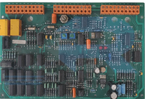
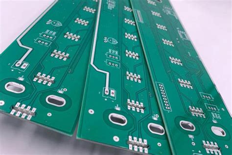
Double Sided PCB Soldering: Reliable Connection Methods

Key Takeaways
Successful double-sided PCB soldering hinges on balancing precision, thermal control, and alignment to ensure reliable PCB joints. For PCB assembly workflows, understanding the interplay between through-hole and surface-mount techniques is critical. Thermal stress management becomes paramount when working with double-sided boards, as uneven heat distribution risks warping or delamination.
Here’s a quick comparison of core methods:
| Technique | Use Case | Key Benefit |
|---|---|---|
| Through-Hole | High-power components | Mechanical stability |
| Surface-Mount | Miniaturized designs | Space efficiency |
For PCBA (Printed Circuit Board Assembly), alignment strategies like fiducial markers or optical inspection systems enhance placement accuracy. Proper tool selection—such as temperature-controlled irons or reflow ovens—reduces defects like cold joints or bridging. Additionally, flux application and solder paste stenciling play pivotal roles in achieving uniform connections across both board layers.
To avoid common errors, prioritize pre-soldering checks for component orientation and pad integrity. Integrating these practices into your PCB assembly process ensures durable, high-performance boards capable of withstanding operational demands.
Through-Hole PCB Soldering Methods
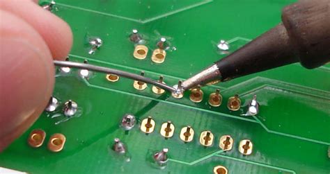
Through-hole soldering remains a cornerstone of PCB assembly for components requiring robust mechanical and electrical connections. This method involves inserting component leads through pre-drilled holes in the board, followed by soldering them to pads on both sides. For double-sided PCBA, ensuring uniform solder fillets on both layers is critical to prevent weak joints. Manual soldering with a temperature-controlled iron works for prototypes, while wave soldering is preferred for high-volume production, as it efficiently coats all leads simultaneously.
Tip: When using wave soldering, maintain a conveyor speed of 1–2 meters per minute to achieve optimal solder penetration without overheating sensitive components.
Thermal management is vital here—excessive heat can delaminate the board or damage nearby parts. Preheating the PCB to 100–120°C before soldering reduces thermal shock and improves solder flow. For boards with dense layouts, staggered lead trimming after soldering minimizes stress on the joints. Always inspect connections under magnification to verify complete wetting and the absence of voids or cracks.
In mixed-technology PCBA (combining through-hole and surface-mount components), solder the through-hole parts first to avoid exposing smaller SMDs to higher temperatures twice. Proper alignment of leads with their respective holes ensures smooth insertion, reducing the risk of bent pins or misaligned traces. For double-sided boards, use temporary adhesives or fixtures to secure components during soldering, especially when working on the secondary side.
Surface-Mount PCB Assembly Tips
Effective PCB assembly of surface-mount devices (SMDs) demands precision and adherence to modern PCBA standards. Unlike through-hole components, SMDs require careful handling due to their compact size and direct placement on board pads. Start by ensuring cleanliness of the PCB surface, as residual flux or debris can compromise solder joint integrity. Use solder paste stencils to apply precise amounts of solder, focusing on even distribution to prevent bridging or voiding during reflow.
When positioning components, automated pick-and-place machines enhance accuracy, especially for high-density designs. For manual assembly, tweezers with anti-static properties are critical to avoid electrostatic discharge damage. Maintain a consistent temperature profile during reflow soldering—rapid heating can cause thermal shock, while uneven cooling may lead to brittle connections.
A key challenge in double-sided PCB assembly is managing component orientation on both layers. Secure smaller SMDs on the secondary side first to prevent displacement when flipping the board. Additionally, leverage low-temperature solder alloys for secondary-side reflow to preserve existing joints. Post-assembly, inspect joints using magnification tools or automated optical inspection (AOI) systems to identify cracks or misalignments.
Integrating these strategies ensures reliable PCBA outcomes, particularly for complex double-sided layouts where thermal and mechanical stresses are amplified. Proper technique minimizes rework and aligns with industry benchmarks for durability and electrical performance.
Thermal Management for Durable PCBs
Effective thermal management is critical for ensuring the longevity and reliability of double-sided PCB assembly (PCBA). During soldering, uneven heat distribution can lead to thermal stress, causing warping, delamination, or cracked joints. To mitigate these risks, engineers prioritize materials with high thermal conductivity, such as FR4 substrates or metal-core boards, paired with thermal vias to dissipate heat between layers.
In PCBA processes, components like power regulators or high-current ICs generate significant heat, necessitating heatsinks or thermally conductive adhesives. For surface-mount devices (SMDs), reflow soldering profiles must balance peak temperatures with exposure time to avoid damaging sensitive parts. Conversely, through-hole components benefit from wave soldering techniques that ensure consistent heat application across both board sides.
Advanced thermal relief patterns in copper traces prevent excessive heat transfer during soldering, while conformal coatings shield circuits from environmental factors. For industrial applications, real-time infrared thermography helps monitor temperature gradients during PCB assembly, enabling adjustments to tooling or工艺流程. By integrating these strategies, manufacturers achieve durable, high-performance PCBA outputs capable of withstanding operational demands.
Transitioning to alignment strategies, precise component placement further enhances thermal efficiency by minimizing heat-trapping layouts.
PCB Alignment Strategies for Precision
Accurate component alignment is critical in PCB assembly to ensure electrical functionality and mechanical stability, particularly in double-sided designs. While thermal stresses and material expansion can shift components during soldering, employing optical alignment systems helps maintain positional accuracy. These systems use high-resolution cameras to map fiducial markers on the board, enabling precise placement of surface-mount devices (SMDs) and through-hole components. For PCBA workflows, combining automated pick-and-place machines with manual adjustments ensures tight tolerances, even for fine-pitch ICs or connectors.
Another key strategy involves using alignment jigs or custom fixtures to secure boards during soldering, minimizing warping caused by uneven heat distribution. Additionally, verifying pad-to-hole ratios and solder mask registration during design prevents misalignment in multilayer PCB assembly. Post-soldering inspection tools, such as automated optical inspection (AOI), further validate alignment integrity by comparing placements against CAD data. By integrating these methods, manufacturers achieve repeatable precision in PCBA processes, reducing rework and enhancing reliability in complex double-sided circuits.
Reliable PCB Joints: Double-Sided Tips
Achieving durable connections in double-sided PCB soldering requires balancing precision with robust thermal management. Unlike single-layer boards, double-sided designs demand careful attention to solder volume and heat distribution to prevent bridging or cold joints. For PCB assembly workflows, technicians often prioritize through-hole component anchoring on one side before addressing surface-mount devices (SMDs) on the reverse. This staggered approach minimizes thermal stress during PCBA processes, especially when reflow soldering is involved.
A critical factor is ensuring pad cleanliness on both board layers. Residual flux or oxidation can weaken joints, particularly in high-density layouts. Using no-clean flux with controlled viscosity helps maintain conductivity while reducing post-soldering residue. For through-hole components, backside soldering techniques—such as manual touch-ups or selective wave soldering—enhance mechanical stability without overheating adjacent SMDs.
Alignment accuracy remains paramount. Misaligned vias or plated through-holes (PTHs) disrupt electrical continuity between layers. Employing optical alignment tools or fiducial markers during PCB assembly ensures layer-to-layer registration within ±0.1mm tolerances. Additionally, monitoring peak reflow temperatures prevents warping, which is critical for maintaining the structural integrity of double-sided PCBA projects. By integrating these strategies, manufacturers achieve reliable interlayer connections that withstand mechanical and environmental stressors.
Step-by-Step Double-Sided Soldering
Executing double-sided PCB soldering requires meticulous planning to ensure electrical continuity and mechanical stability across both layers. Begin by preparing the board with a solder mask to isolate non-conductive areas, followed by applying flux to minimize oxidation. For PCB assembly involving through-hole components, insert leads into plated-through holes (PTHs) and solder one side using a temperature-controlled iron, then flip the board to replicate the process on the reverse.
When working with PCBA designs that include surface-mount devices (SMDs), start by stenciling solder paste onto pads for the first side. Place components using tweezers or a pick-and-place machine, then reflow in an oven. After cooling, secure the board with fixtures to prevent movement before repeating the paste application and component placement for the second layer. Thermal relief patterns are critical here to manage heat distribution during multiple reflow cycles.
A critical step is verifying alignment between layers using optical inspection tools or fiducial markers. For complex layouts, employ PCB assembly techniques like pin-in-paste (PiP) to combine through-hole and SMD soldering in a single reflow cycle. Always inspect joints under magnification for bridging or cold solder, and perform continuity tests to confirm interlayer connections. This systematic approach ensures robust PCBA outcomes, even for high-density double-sided designs.
Essential PCB Soldering Tools Overview
Achieving reliable PCB assembly requires precise selection and application of soldering tools. At minimum, a temperature-controlled soldering iron with interchangeable tips is critical for adapting to different component sizes and thermal requirements. For through-hole components, a desoldering pump or braid ensures clean removal of excess solder during rework. Surface-mount PCBA processes demand tools like fine-tip tweezers and magnifying lenses to handle miniature components accurately.
Thermal management tools, such as preheaters or hot air rework stations, mitigate warping risks in double-sided boards by ensuring even heat distribution. Solder paste applicators and stencils become indispensable for applying precise amounts of lead-free solder in automated workflows. Additionally, a quality flux pen or syringe enhances solder flow while preventing oxidation, particularly in high-density layouts.
For alignment and stability, PCB holders with adjustable clamps secure boards during soldering, minimizing misalignment. Multimeters and continuity testers should follow every PCBA step to verify electrical integrity before finalizing connections. By equipping your workstation with these tools, you establish a foundation for consistent, defect-free soldering across both manual and automated assembly stages.
Avoiding PCB Soldering Common Errors
Even experienced technicians can encounter pitfalls during PCB assembly, particularly with double-sided PCBA. One critical error involves improper thermal management, such as overheating components while soldering one side, which risks damaging traces or delaminating the board. To mitigate this, use a temperature-controlled iron and limit dwell time on each joint. Another frequent issue is solder bridging, where excess solder connects adjacent pads or pins. This is especially problematic in high-density layouts—applying precise solder amounts and leveraging flux to improve flow control can prevent unintended connections.
Misaligned components during PCBA are another common oversight, particularly with surface-mount devices (SMDs). Ensure accurate placement using optical aids or alignment markers before fixing parts permanently. For through-hole components on double-sided boards, insufficient hole fill or uneven solder distribution may weaken joints. Always verify that solder wets both the lead and pad fully, creating a concave fillet. Finally, neglecting post-soldering inspections—such as X-ray imaging for hidden bridges or automated optical inspection (AOI)—can leave latent defects undetected. Pair visual checks with continuity testing to confirm electrical integrity across both board layers, ensuring reliable performance in finished assemblies.
Conclusion
Achieving reliable connections in double-sided PCB soldering hinges on balancing precision, technique, and material knowledge. Whether employing through-hole or surface-mount methods, ensuring robust electrical and mechanical bonds requires attention to thermal profiles, solder alloy selection, and alignment accuracy. For PCB assembly workflows, integrating PCBA best practices—such as preheating boards to mitigate thermal stress and using fiducial markers for layer alignment—can significantly enhance joint durability. Additionally, addressing challenges like solder bridging or void formation demands disciplined tool maintenance and process validation. By prioritizing repeatable methodologies and leveraging advanced tools like reflow ovens or automated optical inspection (AOI), manufacturers can streamline production while maintaining consistency across complex double-sided PCB designs. Ultimately, mastering these strategies ensures assemblies meet both performance benchmarks and long-term reliability demands.
FAQs
How does double-sided soldering affect PCB assembly complexity?
Double-sided soldering increases PCB assembly complexity by requiring precise thermal management and alignment. Components on both layers must undergo sequential or simultaneous heating, demanding controlled processes to prevent warping or solder bridging.
What distinguishes through-hole from surface-mount techniques in PCBA?
Through-hole soldering secures components via drilled holes, ideal for high-stress applications, while surface-mount technology (SMT) in PCBA places parts directly on pads, enabling miniaturization. Both methods may coexist in double-sided designs, necessitating specialized reflow or wave soldering equipment.
How can thermal stress be minimized during double-sided PCB soldering?
Use low-temperature solder alloys and staggered heating cycles to protect existing joints. Ensure adequate thermal relief pads in the design phase to dissipate heat efficiently, reducing risks of delamination or component failure.
What alignment strategies prevent errors in double-sided PCBA?
Optical alignment systems and fiducial markers ensure layer-to-layer precision. For manual setups, guide pins and soldermask registration marks help maintain accuracy during component placement and reflow stages.
Why do some double-sided PCBs require selective soldering?
Mixed-technology boards with heat-sensitive components often need selective soldering to isolate thermal exposure. This targeted approach preserves integrity in PCB assembly while ensuring reliable interlayer connections.
Optimize Your PCB Assembly Process Today
For tailored solutions in double-sided PCBA, advanced tooling, and expert guidance, please click here to explore professional services that elevate your project’s reliability and performance.