Double-Sided Reflow Soldering: A Comprehensive Overview
Introduction
In the ever-evolving world of electronics manufacturing, the demand for more compact, efficient, and high-performance devices has driven the development of advanced soldering techniques. Among these, double-sided reflow soldering has emerged as a critical process for assembling printed circuit boards (PCBs) with components on both sides. This technique allows manufacturers to maximize the use of PCB real estate, enabling the production of smaller, more complex devices without compromising functionality. This article delves into the intricacies of double-sided reflow soldering, exploring its process, advantages, challenges, and applications.
1. What is Double-Sided Reflow Soldering?
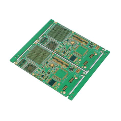
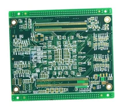
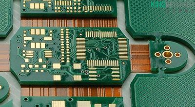
Double-sided reflow soldering is a process used in surface-mount technology (SMT) to attach electronic components to both sides of a PCB. Unlike single-sided reflow, where components are placed and soldered on only one side of the board, double-sided reflow involves two separate soldering cycles—one for each side of the PCB. This method is particularly useful for high-density designs where space is at a premium.
The process typically involves the following steps:
- Stencil Printing: Solder paste is applied to the PCB using a stencil.
- Component Placement: Automated pick-and-place machines position components on the PCB.
- Reflow Soldering: The PCB is passed through a reflow oven, where the solder paste melts and forms permanent solder joints.
- Cooling: The PCB is cooled to solidify the solder joints.
- Flip and Repeat: The PCB is flipped, and the process is repeated for the other side.
2. The Double-Sided Reflow Process in Detail
The double-sided reflow process requires careful planning and execution to ensure the integrity of the solder joints and the components. Below is a detailed breakdown of each step:
2.1 Stencil Printing
The first step in the process is applying solder paste to the PCB. A stencil, typically made of stainless steel, is aligned with the PCB, and solder paste is spread across it using a squeegee. The paste is deposited onto the pads where components will be placed. Precision in this step is crucial, as insufficient or excessive solder paste can lead to defects such as bridging or incomplete solder joints.
2.2 Component Placement
Once the solder paste is applied, components are placed on the PCB using automated pick-and-place machines. These machines use vacuum nozzles to pick up components from reels or trays and place them accurately on the solder paste deposits. For double-sided reflow, components are placed on one side of the PCB first.
2.3 Reflow Soldering
The PCB is then conveyed through a reflow oven, which consists of multiple heating zones. The oven gradually heats the PCB to melt the solder paste, forming solder joints. The temperature profile is carefully controlled to prevent thermal shock, component damage, or solder defects. After reaching the peak temperature, the PCB is cooled to solidify the solder joints.
2.4 Flip and Repeat
After the first side is soldered, the PCB is flipped, and the process is repeated for the other side. This step requires special consideration to ensure that the components on the first side do not fall off or get damaged during the second reflow cycle. Techniques such as using low-temperature solder paste or adhesive can help secure components during the second reflow.
3. Advantages of Double-Sided Reflow Soldering
Double-sided reflow soldering offers several advantages, making it a preferred choice for many electronics manufacturers:
3.1 Increased Component Density
By utilizing both sides of the PCB, manufacturers can significantly increase the component density, enabling the design of smaller and more compact devices. This is particularly important for modern electronics, where space is often limited.
3.2 Improved Performance
Double-sided designs can reduce the length of electrical traces, minimizing signal delays and improving the overall performance of the device. This is especially beneficial for high-speed and high-frequency applications.
3.3 Cost Efficiency
Using both sides of the PCB can reduce the overall size of the board, leading to material savings. Additionally, fewer layers may be required in the PCB design, further reducing costs.
3.4 Design Flexibility
Double-sided reflow soldering allows for greater design flexibility, enabling engineers to optimize the layout for better thermal management, signal integrity, and mechanical stability.
4. Challenges and Considerations
While double-sided reflow soldering offers numerous benefits, it also presents several challenges that must be addressed to ensure successful assembly:
4.1 Component Stability During Second Reflow
One of the primary challenges is ensuring that components on the first side remain securely attached during the second reflow cycle. Components with low thermal resistance or those not designed for high temperatures may detach or shift. To mitigate this, manufacturers can use adhesives, low-temperature solder pastes, or selective soldering techniques.
4.2 Thermal Management
The repeated exposure to high temperatures during the two reflow cycles can stress components and the PCB itself. Careful control of the reflow profile is essential to prevent damage such as warping, delamination, or component failure.
4.3 Solder Paste Compatibility
The solder paste used for the first side must be compatible with the second reflow cycle. If the first side’s solder paste re-melts during the second cycle, it can lead to defects such as tombstoning or bridging. Using solder pastes with different melting points can help address this issue.
4.4 Inspection and Rework
Double-sided PCBs are more challenging to inspect and rework due to the increased complexity and component density. Automated optical inspection (AOI) and X-ray inspection systems are often used to detect defects, but rework may require specialized tools and expertise.
5. Applications of Double-Sided Reflow Soldering
Double-sided reflow soldering is widely used in various industries where compact and high-performance electronics are required. Some common applications include:
5.1 Consumer Electronics
Smartphones, tablets, and wearable devices often use double-sided PCBs to maximize space and functionality.
5.2 Automotive Electronics
Modern vehicles rely on advanced electronics for infotainment, navigation, and safety systems. Double-sided reflow soldering enables the production of compact and reliable automotive PCBs.
5.3 Medical Devices
Medical devices, such as pacemakers and imaging equipment, require high-density PCBs to accommodate complex circuitry in small form factors.
5.4 Industrial Electronics
Industrial control systems, robotics, and IoT devices benefit from the increased component density and performance offered by double-sided reflow soldering.
6. Future Trends and Innovations
As electronics continue to shrink in size and grow in complexity, double-sided reflow soldering is expected to evolve further. Some emerging trends and innovations include:
6.1 Advanced Materials
The development of new solder alloys and PCB materials with improved thermal and mechanical properties will enhance the reliability of double-sided reflow soldering.
6.2 Miniaturization
As components become smaller and more densely packed, manufacturers will need to refine their processes to accommodate micro-sized components and fine-pitch designs.
6.3 Automation and AI
The integration of artificial intelligence and machine learning into soldering processes will enable real-time monitoring and optimization, reducing defects and improving yield.
6.4 Environmentally Friendly Practices
The industry is moving toward lead-free and low-temperature soldering processes to reduce environmental impact and comply with regulations.
Conclusion
Double-sided reflow soldering is a vital technique in modern electronics manufacturing, enabling the production of compact, high-performance devices. While it presents unique challenges, advancements in materials, processes, and technology continue to push the boundaries of what is possible. As the demand for smaller and more complex electronics grows, double-sided reflow soldering will remain a cornerstone of the industry, driving innovation and enabling the next generation of electronic devices.
By understanding the intricacies of this process and addressing its challenges, manufacturers can harness the full potential of double-sided reflow soldering to create cutting-edge products that meet the needs of today’s fast-paced technological landscape.


