Efficient BGA Signal Routing Techniques in PCB Design
Introduction
Ball Grid Array (BGA) packages have become increasingly popular in modern PCB design due to their ability to accommodate high pin counts in a compact form factor. As electronic devices continue to shrink in size while growing in complexity, BGA components offer an effective solution for integrating sophisticated integrated circuits (ICs) with hundreds or even thousands of connections. However, the dense arrangement of pins in BGA packages presents significant challenges for PCB designers, particularly when it comes to signal routing.
This article explores proven techniques for efficiently routing signals from BGA components while maintaining signal integrity, minimizing crosstalk, and ensuring manufacturability. We will examine escape routing strategies, layer stackup considerations, via selection, and advanced routing approaches that can help designers overcome the challenges posed by high-density BGA packages.
Understanding BGA Package Characteristics
Before delving into routing techniques, it’s essential to understand the key characteristics of BGA packages that influence routing decisions:
- Pitch Size: Modern BGAs come in various pitch sizes ranging from 1.0mm down to 0.3mm or smaller. The pitch (distance between ball centers) directly affects routing feasibility.
- Ball Arrangement: BGAs typically have balls arranged in a grid pattern, either fully populated or with depopulated areas. The arrangement may be uniform or staggered.
- Ball Count: High-performance processors and FPGAs can have ball counts exceeding 2000, creating significant routing challenges.
- Power Distribution: BGAs often require multiple power and ground connections that must be properly distributed to maintain stable voltage levels.
Understanding these characteristics helps designers select appropriate routing strategies before beginning the PCB layout process.
Layer Stackup Planning for BGA Routing
Effective BGA routing begins with proper layer stackup design. The stackup should be planned with the following considerations:
- Signal Layers: Allocate sufficient signal layers adjacent to the BGA component to accommodate all required escapes. High-density BGAs may require 8 or more signal layers.
- Power and Ground Planes: Include dedicated power and ground planes to provide low-impedance power distribution and good return paths for high-speed signals.
- Microvia Support: For very fine-pitch BGAs (≤0.5mm), consider using microvias in the stackup to facilitate escape routing.
- Impedance Control: Plan controlled impedance layers for high-speed signals early in the stackup design process.
A typical stackup for a high-density BGA might include:
- Top Layer (Signal)
- Ground Plane
- Signal Layer
- Power Plane
- Signal Layer
- Ground Plane
- Signal Layer
- Bottom Layer (Signal)
Additional layers would be added as needed based on routing density requirements.
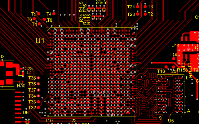
BGA Escape Routing Strategies
Escape routing refers to the process of routing signals from the BGA balls to areas where there is more space for conventional routing. Several strategies exist for efficient BGA escape routing:
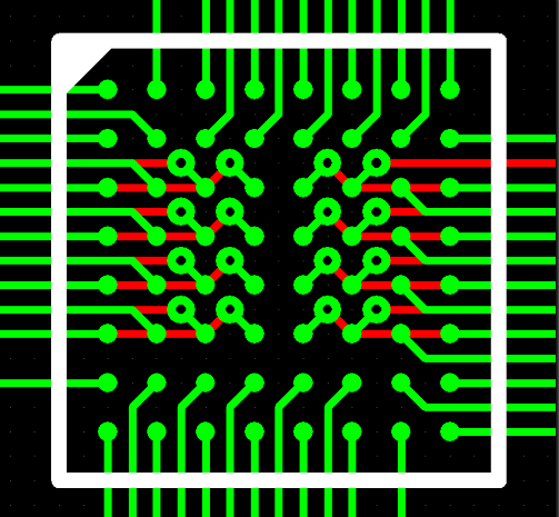
1. Dog-Bone Fanout
The most common escape method uses “dog-bone” patterns where:
- A via is placed adjacent to each BGA ball
- A short trace connects the ball to the via
- The via transfers the signal to an inner layer
This approach works well for pitches down to about 0.8mm with conventional PCB technology.
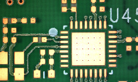
2. Via-in-Pad
For finer pitch BGAs (0.5mm or less), via-in-pad technology becomes necessary:
- Vias are placed directly in the BGA pad
- The via is filled and plated over to create a flat surface for soldering
- This allows maximum utilization of space between balls
Via-in-pad requires more advanced (and expensive) PCB fabrication processes but enables routing of ultra-fine-pitch components.
3. Staggered Via Patterns
When using dog-bone fanouts, staggering vias in alternating rows can improve routing density:
- Odd rows fan out in one direction
- Even rows fan out in the opposite direction
- This creates more space between vias for routing traces
4. Layer-specific Escape
Different signals can be assigned to escape on different layers:
- High-speed signals might escape on top layer for shortest path
- Slower signals can escape on inner layers
- Power and ground connections can use dedicated vias to planes
Via Selection and Placement
Via selection is critical for successful BGA routing:
- Via Size: Choose the smallest via diameter that your PCB manufacturer can reliably produce. Typical sizes range from 0.2mm to 0.3mm for high-density designs.
- Via Type:
- Through-hole vias: Most economical but consume space on all layers
- Blind vias: Connect outer layers to specific inner layers
- Buried vias: Connect inner layers without reaching outer layers
- Microvias: Small vias (typically <0.15mm) for high-density interconnects
- Via Placement:
- Maintain adequate spacing between vias to allow trace routing
- Follow manufacturer’s design rules for via-to-via and via-to-trace spacing
- Consider via aspect ratio (depth to diameter) limitations
Advanced Routing Techniques
Once signals have escaped the BGA area, several techniques can help manage the remaining routing:
1. Differential Pair Routing
For high-speed differential signals:
- Maintain consistent spacing between pair members
- Route pairs symmetrically from the BGA
- Match lengths to maintain timing
- Avoid unnecessary vias which can cause impedance discontinuities
2. Length Matching
For critical parallel buses or clock networks:
- Use serpentine routing to match trace lengths
- Implement matching at the BGA escape area when possible
- Account for via lengths in total length calculations
3. Signal Integrity Considerations
- Maintain proper impedance throughout the route
- Minimize stub lengths when using vias
- Provide adequate ground return paths
- Avoid sharp corners which can cause reflections
4. Power Distribution
- Use multiple vias for power and ground connections to reduce inductance
- Implement proper decoupling capacitor placement near power pins
- Consider split planes or dedicated power layers for different voltage domains
Design Rule Checks for BGA Routing
Implement rigorous design rule checks (DRC) specific to BGA routing:
- Clearance Verification: Ensure adequate spacing between pads, traces, and vias
- Via-to-Via Spacing: Verify compliance with manufacturer capabilities
- Antenna Rule Checks: Identify potential antenna structures in high-frequency designs
- Signal Integrity Rules: Check for impedance discontinuities and return path issues
- Manufacturability Checks: Verify all features meet fabrication and assembly requirements
Practical Tips for Efficient BGA Routing
- Start with Power and Ground: Route power and ground networks first to establish a solid foundation
- Group Related Signals: Route buses and related signals together to maintain organization
- Use Autorouter Strategically: Employ autorouters for non-critical signals after manual routing of critical paths
- Implement Escape Routing Templates: Create reusable patterns for common BGA configurations
- Plan for Rework: Leave some flexibility for last-minute changes or bug fixes
Future Trends in BGA Routing
As BGA packages continue to evolve, several trends are emerging:
- 3D Packaging: Stacked die and through-silicon vias (TSVs) are changing BGA routing requirements
- Advanced Materials: New substrate materials enable finer features and higher densities
- Automated Tools: AI-assisted routing tools are becoming more sophisticated at handling complex BGA escapes
- Embedded Components: Passive components embedded in the PCB substrate free up surface space
Conclusion
Efficient BGA signal routing requires careful planning, appropriate stackup design, and methodical implementation of proven routing strategies. By understanding BGA package characteristics, selecting the right via technologies, and applying systematic escape routing approaches, designers can successfully route even the most challenging high-density BGA components. As package densities continue to increase, staying current with advanced routing techniques and fabrication technologies will remain essential for PCB design success.
The key to efficient BGA routing lies in balancing competing demands: minimizing layer count while ensuring routability, maintaining signal integrity while achieving density goals, and meeting performance requirements while controlling costs. By applying the techniques discussed in this article and continuously adapting to new technologies, PCB designers can overcome the challenges posed by modern BGA components and create robust, high-performance electronic products.


