Efficient PCB Design and Fabrication Techniques for Success
Key Takeaways
When embarking on a project that demands PCB design and fabrication, understanding the foundational elements can significantly impact the overall success. The journey begins with a clear comprehension of the efficiency involved in each stage of the project. Utilizing modern techniques in PCB assembly, also known as PCBA, can dramatically reduce lead times while enhancing product quality. By meticulously choosing materials and employing advanced software for design, engineers can optimize their workflows, fostering an environment conducive to innovation.
Moreover, the importance of rigorous quality control measures cannot be overstated. Ensuring that each component meets the strictest standards transcends mere compliance; it is instrumental in achieving longevity and reliability in circuits. Industry experts suggest adopting a holistic approach to quality management that encompasses every phase of manufacturing.
As we look toward the future, it is essential to keep abreast of emerging trends and technologies shaping PCB design and fabrication processes. These developments promise not only to refine traditional methods but also to unlock new avenues for enhanced functionality. The integration of automation and smart technology within production lines heralds a new era for manufacturers aiming for superior efficiency and effectiveness.
“Incorporating innovative practices and staying informed about industry trends are key ingredients for thriving in PCB projects.”
Adapting these insights into your strategy can set you apart in a competitive landscape, leading your projects toward greater success in today’s fast-paced electronics market.
Introduction to PCB Design and Fabrication
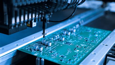
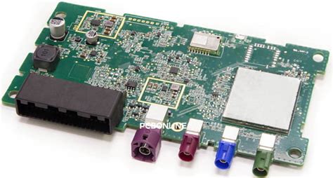
The world of PCB design and fabrication is crucial for the development of modern electronic devices. Understanding the nuances of this field can significantly impact the success of various projects. At its core, PCB assembly—often abbreviated as PCBA—involves transforming conceptual designs into functional electronic solutions. The journey begins with intricate designs that must be meticulously crafted using advanced software tools to ensure that all components fit together seamlessly. Once the design is finalized, the fabrication process comes into play.
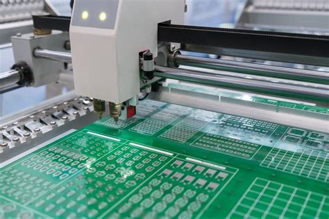
During fabrication, materials such as copper, fiberglass, and solder mask are combined to create a printed circuit board that matches the specifications outlined in the design phase. This process demands precision, as even minor errors can lead to significant delays and increased costs. Therefore, integrating innovative techniques—like automated assembly processes and advanced testing methodologies—can help streamline production timelines while enhancing overall quality.
Moreover, implementing effective quality control measures throughout both design and fabrication phases is paramount. These measures not only ensure compliance with industry standards but also contribute to reducing waste and rework costs in PCB assembly processes. As technology continues to evolve, embracing new trends and innovations in PCB manufacturing becomes essential for maintaining a competitive edge in a global market that demands efficiency and high-quality products. By focusing on these aspects, designers and manufacturers can set themselves up for long-lasting success in their electronic projects.
The Importance of Efficiency in PCB Projects
Efficiency in PCB design and fabrication is crucial for the success of any electronic project. In an industry where timeliness and cost-effectiveness are paramount, optimizing processes can significantly enhance the performance and profitability of electronic products. By focusing on efficiency, teams can minimize waste, reduce production time, and ensure high-quality PCB assembly (PCBA).
One pivotal aspect in achieving this efficiency involves adopting advanced tools and methodologies during the design phase. Utilizing automated design software can help identify potential issues early, enabling designers to make informed decisions that streamline their layouts. Furthermore, implementing design rules tailored for high-density interconnects (HDI) can maximize the use of space on a circuit board while maintaining electrical performance.
The fabrication process also benefits from efficiency-focused innovations. For instance, leveraging flexible circuit board technology allows for reduced material costs and simplified assembly procedures. This can lead to faster turnarounds on prototypes and ultimately lower the overall expenditure in project execution.
To illustrate these points, consider a simplified comparison table:
| Aspect | Traditional Approach | Efficient Approach |
|---|---|---|
| Design Time | Longer due to revisions | Streamlined with automated checks |
| Material Waste | Higher due to excess | Lower with optimized layouts |
| Production Speed | Slower with manual steps | Increased through automation |
| Quality Assurance | Reactive inspections | Proactive quality controls |
By prioritizing these innovative techniques in both PCB design and its subsequent fabrication, teams not only enhance their outcomes but also position themselves favorably within a competitive landscape. As projects become more complex, integrating efficiency will be key to ensuring successful PCBA outcomes that meet market demands effectively.
Innovative Techniques in PCB Design
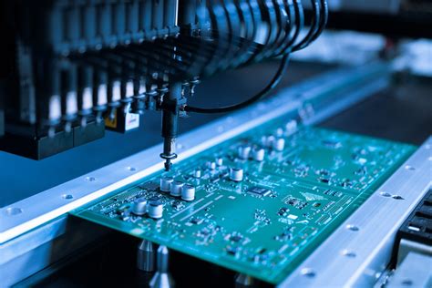
The advancement of technology has significantly influenced PCB design and its associated processes, introducing innovative techniques that streamline workflows and improve outcomes. One key aspect is the integration of software tools that facilitate 3D modeling and simulation, allowing designers to visualize their PCB assemblies before fabrication. This proactive approach not only minimizes potential design flaws but also enhances the overall efficiency of the pcb assembly process. Furthermore, the adoption of automation in aspects such as component placement and soldering contributes to greater accuracy and speed during PCBA (Printed Circuit Board Assembly). Coupled with the use of advanced materials, these techniques can significantly reduce manufacturing costs while maintaining high-quality standards. Emphasizing collaboration between design teams and manufacturer counterparts ensures that the transition from concept to reality is seamless, fostering innovation at every stage. As a result, integrating these innovative design practices can substantially elevate the quality of electronic projects, ultimately leading to successful outcomes in a competitive market landscape.
Streamlining the Fabrication Process
To achieve success in PCB design and fabrication, it is crucial to streamline the fabrication process effectively. A fundamental aspect of this is optimizing the transition from design to PCB assembly. The use of advanced software tools can aid designers in creating more efficient layouts that reduce manufacturing time and costs. By employing techniques such as design for manufacturability (DFM), engineers can identify potential issues early in the design phase, thus minimizing errors during production. Additionally, integrating automated processes into PCBA can significantly enhance efficiency. Automation not only speeds up assembly but also ensures a higher level of consistency and precision in the final product, which is vital for maintaining quality standards.
Moreover, adopting modular designs allows flexibility and easier troubleshooting during the manufacturing phase. This approach facilitates quicker iterations and adaptations that align with evolving project requirements. Implementing robust communication channels between design and manufacturing teams fosters collaborative problem-solving, leading to innovative solutions that further streamline operations. Ultimately, by embracing these strategies within the fabrication process, organizations can improve overall productivity and quality while reducing costs, paving the way for successful electronic projects that thrive in a competitive industry landscape.
Quality Control Measures in PCB Manufacturing
Quality control in PCB manufacturing is essential to ensure that the final product meets stringent industry standards and client expectations. Implementing effective quality control measures throughout the PCB design and fabrication processes can significantly mitigate risks associated with defects and enhance the reliability of pcb assembly. A critical aspect of quality assurance involves regular inspections and tests, such as visual examination, automated optical inspection (AOI), and electrical testing, which collectively help identify potential issues early in the production cycle. Moreover, establishing standard operating procedures (SOPs) and continually training staff to adhere to these guidelines can foster a culture of quality and accountability. Employing advanced techniques, such as statistical process control (SPC) and root cause analysis (RCA), allows manufacturers to analyze processes systematically, enabling them to optimize operations effectively while maintaining high standards. Ultimately, focusing on these measures not only increases consumer confidence but also enhances overall production efficiency within the realm of pcba. By prioritizing quality at every stage of manufacturing, companies can significantly reduce waste, lower costs, and achieve greater customer satisfaction in an increasingly competitive marketplace.
Case Studies: Successful PCB Projects and Their Techniques
Understanding successful PCB projects involves examining concrete examples where efficiency and innovation played crucial roles. For instance, one prominent case involved a consumer electronics company that sought to cut costs and enhance performance by optimizing their PCB assembly (PCBA) process. By implementing advanced design software that allowed for real-time simulation and adjustments, engineers were able to reduce the number of layers in their PCB design, resulting in faster production times without sacrificing quality. This shift not only streamlined the design but also significantly minimized materials waste—a key factor in sustainability efforts within the industry. Another fascinating case highlights an automotive manufacturer that embraced modular PCB fabrication techniques. By incorporating flexible circuits, they managed to reduce overall weight while increasing the ease of integration with various automotive systems. This innovative approach not only improved overall efficiency but also set a new standard for safety and performance in their electronic systems, ultimately contributing to enhanced vehicle reliability. Such case studies illustrate how adopting innovative techniques in PCB assembly can lead to remarkable advancements, setting benchmarks for future projects within the electronics sector.
Future Trends in PCB Design and Fabrication
As technology continues to advance, the field of PCB design and fabrication is witnessing transformative trends that promise to enhance both the efficiency and effectiveness of electronic projects. One of the most prominent trends is the increasing incorporation of automation in pcb assembly, which streamlines the manufacturing process and minimizes human error. This shift towards automation enables companies to scale production while maintaining high standards of quality, crucial for today’s fast-paced market demands. Additionally, advancements in materials science are leading to the development of more innovative substrates that improve performance and reliability in high-frequency applications. The move towards more compact designs is also influencing the trend; companies are focusing on techniques such as multilayer PCBs that allow for increased functionality without expanding physical space. Moreover, embracing sustainable practices such as environmentally friendly materials and energy-efficient processes is becoming essential as global demands for sustainability rise. As these trends evolve, they offer significant opportunities for manufacturers to improve their workflows while ensuring they remain competitive in a rapidly changing industry. Overall, understanding and adapting to these future trends will be vital for achieving success in PCB fabrication and ensuring high-quality pcba outcomes.
Conclusion: Embracing Innovation for PCB Success
In today’s rapidly evolving electronics landscape, the significance of embracing innovation in PCB design and fabrication cannot be overstated. As the demand for more compact and efficient electronic devices rises, so does the complexity of PCB assembly processes. Companies must remain agile and open to adopting cutting-edge techniques that not only enhance production speed but also ensure superior quality in the resulting PCBA (Printed Circuit Board Assembly). Implementing automated tools and advanced software for designing intricate layouts can drastically reduce lead times and minimize errors. Additionally, aligning manufacturing processes with the latest advancements—such as 3D printing for prototyping or the incorporation of smart technologies in manufacturing lines—can significantly boost efficiency. The industry’s future hinges on those who are willing to innovate; organizations that invest in research and development will not only keep pace with competitors but also lead the charge toward a more efficient and sustainable design and fabrication environment. Ultimately, embracing these innovations is essential for achieving long-term success in the PCB design sector, ensuring that businesses remain relevant amid changing technological demands.
Conclusion: Embracing Innovation for PCB Success
In the rapidly evolving world of electronics, embracing innovation in PCB design and fabrication is critical for success. The integration of advanced techniques not only enhances the efficiency of PCB assembly processes but also significantly improves the quality of the finished product. As we’ve explored throughout this article, implementing strategies such as automated design tools, multi-layer boards, and enhanced testing protocols in PCBA can streamline workflows, reduce production times, and minimize errors. These methods allow designers and engineers to respond more agilely to the demands of the ever-changing market while maintaining a focus on reliability and functionality. Furthermore, fostering a culture of continuous improvement and leveraging emerging technologies can lead to revolutionary breakthroughs in PCB manufacturing. Hence, by prioritizing innovation and adopting state-of-the-art practices, businesses can establish a competitive edge that not only drives their success but also contributes to the overall advancement of the industry.
FAQs
What is PCB assembly?
PCB assembly, or PCBA, refers to the process of attaching electronic components to a printed circuit board (PCB). This process can significantly influence the performance and reliability of the final electronic product.
Why is efficiency important in PCB design?
Efficiency in PCB design leads to reduced production costs, shorter lead times, and improved product quality. Optimizing designs ensures that resources are utilized effectively, enhancing overall project success.
What innovative techniques can improve PCB fabrication?
Some innovative techniques include utilizing advanced software tools for layout optimization, employing automated assembly systems for increased precision, and implementing real-time quality control measures during the fabrication process.
How can I ensure quality in PCB manufacturing?
To ensure quality, implement strict quality control measures such as thorough testing during various production stages, using high-quality materials, and adhering to industry standards throughout the pcb assembly process.
What are some examples of successful PCB projects?
Successful projects often leverage innovative design principles and efficient fabrication techniques. Industry leaders have successfully implemented advanced technologies that enhance product functionality while reducing manufacturing time.
Explore More on PCB Assembly
For further insights into optimizing your PCB assembly, please click here: Andwin PCB Assembly.