Electrical Clearance in PCB Design: Ensuring Safety and Reliability
Introduction
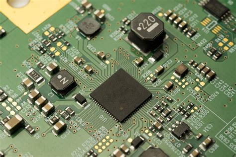
Printed Circuit Board (PCB) design involves numerous critical considerations, among which electrical clearance stands as one of the most fundamental safety requirements. Electrical clearance, often referred to as the “safe distance” between conductive elements on a PCB, plays a vital role in preventing electrical shorts, minimizing leakage currents, and ensuring long-term reliability of electronic devices. This article explores the concept of PCB electrical safety distances, examining the governing principles, calculation methods, international standards, and practical implementation strategies that engineers must consider during PCB design.
Understanding Electrical Clearance
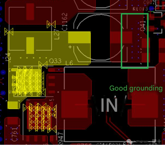
Electrical clearance in PCB design refers to the shortest distance through air between two conductive parts that ensures safe operation under normal and fault conditions. This separation distance prevents several potential issues:
- Dielectric breakdown: When the voltage between conductors exceeds the dielectric strength of air (approximately 3 kV/mm), ionization occurs, potentially leading to arcing.
- Surface tracking: Contamination or moisture on the PCB surface can create conductive paths between traces if clearances are insufficient.
- Manufacturing tolerances: Adequate clearance compensates for variations in PCB fabrication processes.
The required clearance depends on multiple factors including working voltage, environmental conditions, pollution degree, and material characteristics. Unlike creepage distance (the shortest path along the surface between conductors), clearance measures the straight-line air gap between conductive elements.
Key Factors Affecting Electrical Clearance Requirements
1. Operating Voltage
The potential difference between conductors directly influences the minimum required clearance. Higher voltages demand greater separations to prevent dielectric breakdown. The relationship isn’t strictly linear due to the non-uniform electric field distribution in practical PCB layouts.
2. Altitude Considerations
At higher altitudes, reduced air density lowers dielectric strength, necessitating increased clearances. Standards typically specify correction factors for operation above 2000 meters.
3. Pollution Degree
International standards classify operating environments into four pollution degrees:
- Degree 1: Clean environments with no conduction or temporary conductivity caused by condensation
- Degree 2: Normally only non-conductive pollution occurs
- Degree 3: Conductive pollution occurs or dry non-conductive pollution becomes conductive due to condensation
- Degree 4: Persistent conductivity caused by dust, rain, or other wet conditions
Higher pollution degrees require greater clearances to prevent surface tracking.
4. Material Groupings
PCB materials are classified into four groups (I, II, IIIa, IIIb) based on their Comparative Tracking Index (CTI), which measures resistance to surface tracking. Materials with lower CTI values (poorer tracking resistance) require larger clearances.
5. Overvoltage Category
Equipment categories (I-IV) define the severity of transient overvoltages the system might experience, influencing clearance requirements:
- Category I: Signal-level equipment
- Category II: Portable or pluggable equipment
- Category III: Fixed installations with robust distribution systems
- Category IV: Primary supply level equipment
International Standards and Regulations
Several key standards govern PCB electrical clearance requirements:
1. IPC-2221 and IPC-2222
The IPC-2221 generic standard and IPC-2222 sectional standard for rigid PCBs provide tables for minimum electrical clearance based on voltage and environmental conditions. These standards form the foundation for most commercial PCB designs.
2. IEC 60950-1 and IEC 62368-1
These international safety standards for information technology and audio/video equipment specify clearance requirements based on working voltage, pollution degree, and material group. IEC 62368-1 is gradually replacing IEC 60950-1 as the prevailing standard.
3. UL 61010-1
For measurement, control, and laboratory equipment, this standard outlines clearance requirements with particular attention to operator safety.
4. Automotive Standards
Automotive applications follow additional standards like ISO 6469 and various OEM specifications that often impose more stringent requirements than commercial standards due to harsh operating environments.
Calculation Methods for Electrical Clearance
1. Standard Table Lookup
Most standards provide tables listing minimum clearances based on voltage and environmental conditions. For example, IPC-2221 provides basic clearance requirements:
| Voltage (V) | Internal Conductors (mm) | External Conductors (mm) |
|---|---|---|
| 0-15 | 0.05 | 0.1 |
| 16-30 | 0.05 | 0.1 |
| 31-50 | 0.1 | 0.6 |
| 51-100 | 0.15 | 0.6 |
| 101-150 | 0.2 | 0.6 |
| 151-170 | 0.25 | 0.6 |
| 171-250 | 0.3 | 1.2 |
| 251-300 | 0.4 | 1.2 |
| 301-500 | 0.55 | 2.4 |
Note: Values are examples only – consult current standards for precise requirements
2. Empirical Formulas
Some standards provide formulas for calculating clearance. The IEC 60664-1 standard offers:
Clearance (mm) = (Working Voltage × Material Factor × Environmental Factor) + Fixed Margin
Where factors account for altitude, pollution degree, and overvoltage category.
3. Peak Voltage Considerations
For circuits with significant transient voltages or high-frequency signals, clearance should be based on peak rather than RMS voltage values.
Practical Implementation Strategies
1. Layer Stackup Planning
Proper layer arrangement can help manage clearance requirements:
- Place high-voltage circuits on inner layers where pollution risk is lower
- Maintain greater separations on outer layers exposed to environmental contaminants
- Use ground planes between high-voltage layers to provide shielding
2. Component Placement
- Group components by voltage level to minimize high-voltage clearance requirements
- Orient high-voltage components to maximize natural separations
- Consider three-dimensional clearances between tall components
3. Routing Techniques
- Avoid parallel runs of high-voltage differential pairs
- Use curved rather than right-angle traces to reduce field concentration
- Implement tear-dropping at pad connections to minimize sharp points
4. Board Features for Enhanced Safety
- Incorporate slotting or cutouts between high-voltage areas
- Use solder mask strategically (though it doesn’t replace proper clearance)
- Implement guard rings around sensitive high-impedance nodes
Special Considerations
1. High Voltage Applications
For voltages above 1 kV, additional precautions become necessary:
- Field grading techniques to manage electric field distribution
- Corona discharge prevention through smooth conductors
- Partial discharge considerations for long-term reliability
2. High Frequency Signals
At RF frequencies, clearance affects impedance control and crosstalk:
- Maintain consistent spacing for controlled impedance lines
- Consider electromagnetic coupling in addition to basic clearance
- Account for potential standing wave voltage maxima
3. Mixed-Signal Designs
Combining high-voltage and sensitive low-voltage circuits requires:
- Careful partitioning of board areas
- Appropriate isolation techniques
- Attention to return path management
Verification and Testing
1. Design Rule Checks (DRC)
Modern PCB design software includes DRC functions to verify clearances:
- Set appropriate clearance rules for different net classes
- Implement different rules for inner vs. outer layers
- Account for manufacturing tolerances in rule definitions
2. Prototype Testing
- Hi-pot testing to verify dielectric withstand capability
- Insulation resistance measurements
- Environmental stress testing (humidity, thermal cycling)
3. Production Controls
- Regular process capability verification
- Microsection analysis for critical clearances
- Automated optical inspection (AOI) for clearance verification
Future Trends and Challenges
1. Miniaturization Pressures
As electronics continue shrinking, maintaining adequate clearances becomes increasingly challenging, particularly for:
- Wearable and implantable devices
- High-density power electronics
- Advanced packaging technologies
2. New Materials
Emerging substrate materials with higher dielectric strengths may allow reduced clearances, but require careful evaluation of:
- Long-term reliability
- Environmental resistance
- Manufacturing compatibility
3. Higher Voltage Applications
Growing demand in areas like electric vehicles and renewable energy systems drives need for:
- Better clearance prediction methods
- Advanced simulation tools
- Improved testing methodologies
Conclusion
Electrical clearance remains a fundamental aspect of PCB design that directly impacts product safety, reliability, and regulatory compliance. While standards provide essential guidance, effective implementation requires thoughtful consideration of the specific application context, operating environment, and manufacturing realities. As electronic systems continue evolving in complexity and performance demands, the importance of proper clearance design only grows more critical. By understanding the underlying principles, applying appropriate calculation methods, and implementing robust verification processes, designers can ensure their PCBs meet all necessary safety requirements while achieving optimal performance and reliability.
The ongoing development of design tools, materials, and manufacturing processes will continue to shape clearance practices, but the fundamental goal remains unchanged: to create safe, reliable electronic products through proper attention to electrical isolation requirements. In an era of increasingly interconnected and power-dense electronics, meticulous attention to PCB electrical clearance stands as an essential discipline for all electrical engineers and PCB designers.