Electromagnetic Compatibility and PCB Design Constraints
1. Introduction
Electromagnetic Compatibility (EMC) is a critical aspect of modern electronic design, ensuring that electronic devices operate as intended without causing or suffering from electromagnetic interference (EMI). Printed Circuit Board (PCB) design plays a pivotal role in achieving EMC compliance. Poor PCB layout can lead to signal integrity issues, radiated emissions, and susceptibility to external noise, all of which can degrade system performance.
This article explores the relationship between EMC and PCB design, highlighting key constraints and best practices to mitigate EMI. Topics include grounding strategies, signal integrity management, component placement, and routing techniques that enhance EMC performance.
2. Fundamentals of Electromagnetic Compatibility (EMC)
EMC consists of two main aspects:
- Emissions – The generation of electromagnetic energy by a device, which may interfere with other systems.
- Immunity/Susceptibility – The ability of a device to function correctly in the presence of external electromagnetic disturbances.
EMC standards (e.g., FCC, CISPR, IEC) define acceptable emission levels and immunity thresholds. Non-compliance can result in product recalls, legal penalties, or market rejection.
2.1 Sources of EMI in PCBs
- High-frequency signals (clock lines, switching power supplies)
- Poor grounding (ground loops, high impedance return paths)
- Crosstalk (unwanted coupling between traces)
- Radiated emissions (antenna-like structures formed by traces)
3. PCB Design Constraints for EMC Compliance
3.1 Grounding Strategies
Proper grounding is essential for minimizing EMI. Common techniques include:
- Single-Point Grounding – Used in low-frequency circuits to avoid ground loops.
- Multi-Point Grounding – Preferred for high-frequency designs to reduce ground impedance.
- Ground Planes – A solid ground plane beneath signal layers provides a low-impedance return path and reduces radiation.
Best Practices:
- Avoid splitting ground planes unless necessary (e.g., analog/digital separation).
- Use stitching vias to connect ground planes in multilayer PCBs.
- Minimize ground loop areas by keeping return paths short.
3.2 Power Distribution Network (PDN) Design
A well-designed PDN ensures stable power delivery while minimizing noise.
- Decoupling Capacitors – Placed near IC power pins to suppress high-frequency noise.
- Power Plane Segmentation – Isolate noisy power domains (e.g., digital vs. analog).
- Low-Impedance Paths – Use wide traces or power planes to reduce inductance.
3.3 Signal Integrity and Routing Techniques
Signal integrity issues (reflections, crosstalk) can lead to EMI problems.
- Controlled Impedance Routing – Match trace impedance to source/load (e.g., 50Ω for RF lines).
- Differential Pair Routing – Minimizes EMI by canceling out common-mode noise.
- Trace Length Matching – Critical for high-speed signals (e.g., DDR, USB).
- Avoid Sharp Corners – Use 45° or curved traces to reduce impedance discontinuities.
3.4 Component Placement for EMC
Strategic component placement reduces EMI coupling.
- Partitioning – Separate noisy (digital, switching) and sensitive (analog, RF) circuits.
- Shielding – Use metal cans or conductive coatings for high-radiation components.
- Clock Signal Management – Keep clock traces short and away from sensitive areas.
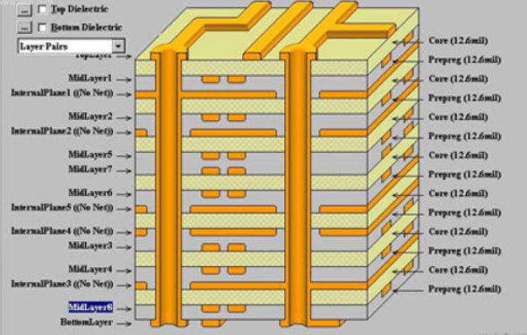
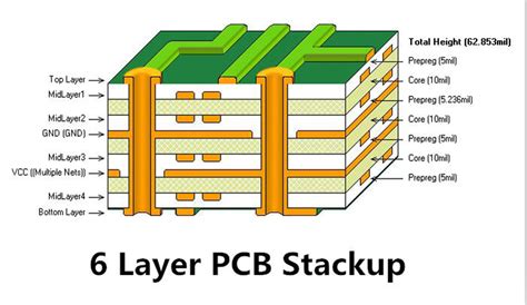
3.5 Layer Stackup Considerations
Multilayer PCBs offer better EMC performance than two-layer designs.
- Recommended Stackup:
- Layer 1: Signal (top)
- Layer 2: Ground plane
- Layer 3: Power plane
- Layer 4: Signal (bottom)
- Shielding Layers – Additional ground layers can contain EMI.
4. Common EMC Failures and Mitigation Techniques
4.1 Radiated Emissions
Cause: High-frequency signals acting as antennas.
Solution:
- Use shorter traces.
- Implement proper grounding.
- Add ferrite beads or filters.
4.2 Conducted Emissions
Cause: Noise coupling into power lines.
Solution:
- Use EMI filters on power inputs.
- Implement proper decoupling.
4.3 Crosstalk
Cause: Adjacent traces coupling capacitively/inductively.
Solution:
- Increase trace spacing.
- Use guard traces or ground shielding.
5. Simulation and Testing for EMC Compliance
5.1 Pre-Layout Simulation
- Signal Integrity Analysis (e.g., HyperLynx, Ansys SIwave)
- Power Integrity Analysis (identify PDN resonances)
5.2 Post-Layout Testing
- Near-Field Probes (detect localized emissions)
- EMI Chambers (measure radiated emissions)
- Conducted Emission Tests (validate power line noise)
6. Conclusion
Achieving EMC in PCB design requires a systematic approach, incorporating proper grounding, power distribution, signal routing, and shielding techniques. By adhering to these constraints, designers can minimize EMI risks and ensure compliance with regulatory standards.
Future trends, such as higher-speed digital interfaces (PCIe 5.0, DDR5) and IoT devices, will further challenge EMC design, necessitating advanced simulation tools and innovative layout strategies.