Electronic inkjet printing technology promotes the development of PCB
From the current and future application and development prospects, the application of inkjet printing technology of fully printed electronics in PCB is mainly reflected in the following three aspects: application in pattern transfer; application in embedded passive components; application in fully printed electronics (including packaging) that directly forms lines and connections. These applications will bring revolutionary changes and progress to the PCB industry.
Application in PCB pattern transfer: mainly reflected in 4 aspects
The application of inkjet printing technology in PCB pattern transfer is mainly in 4 aspects: anti-corrosion, anti-plating, solder mask and characters. Since the process of inkjet printing to form anti-corrosion patterns and anti-plating patterns is basically the same, and the solder mask patterns and character patterns formed by inkjet printing are very close, therefore, it is divided into two parts below: forming anti-corrosion (anti-plating) patterns and forming solder mask/character patterns for a brief review.
1.Application in the formation of anti-corrosion/anti-plating graphics
Using a digital inkjet printer to directly print the anti-corrosion agent (anti-etching ink) on the inner layer (or outer layer) on the board, you can get an acidic or alkaline anti-etching agent pattern. After UV (ultraviolet) light curing, you can etch and remove the film to obtain the required circuit pattern of the inner layer. Similarly, the process of anti-plating graphics is basically the same.
Using digital inkjet printing technology and processes to obtain anti-corrosion/anti-plating graphics not only reduces the production process of photographic negatives, but also avoids the process of exposure and development. The benefits are saving site and space, significantly reducing material consumption (especially negatives and equipment, etc.), shortening product production cycles, reducing environmental pollution, and reducing costs. At the same time, more importantly, it significantly improves the position of the graphics and the alignment between layers (especially eliminating the dimensional deviation caused by the size change of the negative and the exposure alignment), which is extremely beneficial for improving the quality of multi-layer PCB boards and increasing the product qualification rate. Like laser direct imaging (LDI), it can shorten the PCB production cycle and improve product quality, which is an important reform and progress in PCB industry technology.
The graphic transfer technology using digital inkjet printing has the least processing steps (less than 40% of traditional technology), the least equipment and materials, and the shortest production cycle. Therefore, it has the most significant energy-saving and emission-reduction effects, and the lowest environmental pollution and cost.
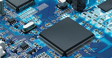
2.Application in the formation of solder mask/character graphics
Similarly, a digital inkjet printer is used to directly print solder mask (solder mask ink) or character ink directly onto the PCB board, and after UV light curing, the final required solder mask graphics and character graphics are obtained.
The use of digital inkjet printing technology and process to obtain solder mask and character graphics has significantly improved the position accuracy of solder mask and character graphics of PCB products, which is also extremely beneficial for improving the quality of PCB boards and increasing product qualification rates. Application in embedded passive components: production of higher-end products
At present, the methods of embedding passive components are mostly realized by using copper clad laminates (CCL) containing resistors/capacitors or screen printing related inks, but these methods not only have many complex processes, long cycles, many equipment and occupy a lot of space, but also have large deviations in product performance, making it difficult to produce high-end products. More importantly, the processing consumes a lot of energy and produces a lot of pollution, which is not conducive to environmental protection. The use of inkjet printing technology to realize the method of embedding passive components will greatly improve these situations.
The application of inkjet printing in embedded passive components refers to the inkjet printer directly printing the conductive ink and other related inks used as passive components to the set position inside the PCB, and then undergoing UV light treatment or drying/sintering treatment to form a PCB product with embedded passive components.
The passive components mentioned here refer to resistors, capacitors and inductors (now developed to embedded active components, such as system packaging).
Due to the development of high density and high frequency of electronic products, more and more passive components are needed to minimize the distortion and noise caused by crosstalk (inductive reactance, capacitive reactance), etc. At the same time, due to the increasing number of passive components, not only the area occupied is increasing, but also the number of welding points is increasing, which has become the biggest factor in the failure rate of industrial electronic products. In addition, the secondary interference generated by the loop formed by surface mounted passive components is increasingly threatening the reliability of electronic products. Therefore, embedding passive components in PCB to improve the electrical performance of electronic products and reduce the failure rate has begun to become one of the mainstream products in PCB production.
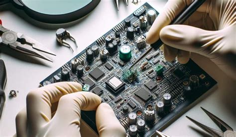
About the principles and methods of embedding passive components in PCB.
Generally speaking, the passive components of embedded resistors, capacitors and inductors, except for the common capacitor placed between the electric/ground layer, are mostly placed on the second layer and the second to last layer (n-1) of the multi-layer PCB.
The resistor conductive glue (ink) used as a resistor is sprayed onto the set position of the inner layer sheet (etched) of the PCB using an inkjet printing device, and the two ends of the bottom are connected by etched wires (open circuit), baked, tested, and then pressed into the PCB board.
Similarly, the capacitor conductive glue (ink) used as a capacitor is sprayed onto the copper foil at the preset position using an inkjet printer, dried and/or sintered, and then sprayed with a layer of conductive ink containing silver, etc., and then dried and/or sintered, and then laminated (inverted) and etched to form both the capacitor and the inner layer circuit.
In electronic products and electronic equipment, the number of inductors used is much less than that of resistors and capacitors.
Similarly, the conductive ink (forming the center electrode) and the inductor material ink are formed into a high inductance dielectric layer using an inkjet printer, and then the conductive ink is sprayed on the high inductance dielectric layer to form a coil.
Application in direct formation of circuit graphics: Two major problems need to be solved
Inkjet printing directly forms circuits, which means that the inkjet printer directly uses conductive ink to print on the substrate (without copper foil) to form conductive circuits and graphics. Fully printed electronics technology means that the entire printed circuit board formation process is completed by inkjet printing technology. At present, fully printed electronics technology is under engineering development and research, but it will soon be promoted and applied.
At present, the main problems of fully printed electronics technology are:
1. Develop advanced inkjet printers for industrialization (large-scale production), especially super inkjet printing equipment; 2. Develop advanced inkjet inks for industrialization, especially various metal nano-level inks, such as silver, copper and gold nano-level inks.
At present, inkjet printing technology is being developed to produce multi-layer printed circuit boards, system packages (SIPs), etc. For example, the super inkjet equipment and silver nano-inks developed by the Japan Advanced Industrial Science and Technology Research Institute are used to directly form multi-layer circuit boards. The process is to use a super inkjet printer to print silver nano-ink onto a copper-free substrate to form a flat circuit layer, and then print connecting bumps on this plane for interlayer connection, and then form an insulating layer between layers, and then form the second layer of circuits on the insulating layer, and so on, to form a multi-layer circuit board with the required number of layers, that is, a fully printed electronic PCB.

