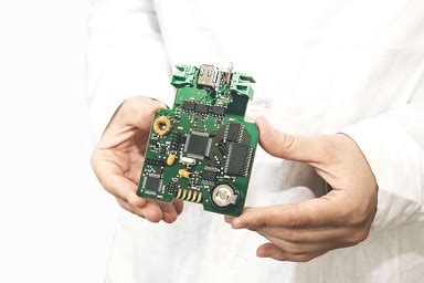
Electronics pcb manufacturing
Advances In PCB Manufacturing Technology
The field of electronics has witnessed remarkable advancements over the past few decades, and one of the pivotal areas contributing to this progress is Electronics pcb manufacturing. As the backbone of modern electronic devices, PCBs have evolved significantly, driven by the relentless pursuit of miniaturization, enhanced performance, and cost efficiency. The advances in PCB manufacturing technology have not only revolutionized the electronics industry but have also paved the way for innovative applications across various sectors.
To begin with, one of the most notable advancements in PCB manufacturing is the development of High-Density Interconnect (HDI) technology.
HDI PCBs are characterized by their higher wiring density per unit area compared to traditional PCBs. This is achieved through the use of microvias, finer lines, and spaces, as well as thinner materials. The adoption of HDI technology has enabled the production of smaller, lighter, and more powerful electronic devices, which is particularly crucial in the consumer electronics market. For instance, smartphones, tablets, and wearable devices have all benefited from the compact and efficient design facilitated by HDI PCBs.
In addition to HDI technology, the advent of flexible PCBs has also marked a significant milestone in the industry.
Flexible PCBs, or flex circuits, are designed to bend and fold, allowing for greater design versatility and space-saving capabilities. This flexibility is particularly advantageous in applications where space constraints and complex geometries are prevalent, such as in medical devices, automotive electronics, and aerospace systems. The ability to conform to various shapes and contours without compromising performance has made flexible PCBs an indispensable component in modern electronic design.
Moreover, the integration of advanced materials has further propelled PCB manufacturing technology.
The use of materials such as polyimide, liquid crystal polymer (LCP), and metal core substrates has enhanced the thermal management, signal integrity, and overall reliability of PCBs. These materials offer superior performance characteristics compared to traditional FR-4 substrates, making them ideal for high-frequency and high-power applications. As electronic devices continue to demand higher performance and efficiency, the adoption of advanced materials in PCB manufacturing is expected to grow.
Another significant advancement in PCB manufacturing is the implementation of additive manufacturing techniques, commonly known as 3D printing.
3D printing has introduced a new dimension to PCB fabrication by enabling the creation of complex geometries and multi-layered structures with unprecedented precision. This technology allows for rapid prototyping and customization, reducing the time and cost associated with traditional manufacturing processes. Furthermore, 3D printing has the potential to revolutionize the production of PCBs for specialized applications, such as in the development of custom sensors and IoT devices.
Furthermore, the integration of automation and artificial intelligence (AI) in PCB manufacturing processes has led to increased efficiency and precision.
Automated optical inspection (AOI) systems, for example, utilize AI algorithms to detect defects and ensure quality control during the production process. This not only enhances the reliability of PCBs but also reduces the likelihood of human error. Additionally, AI-driven design tools have streamlined the PCB design process, enabling engineers to optimize layouts and predict potential issues before fabrication.
In conclusion, the advances in PCB manufacturing technology have significantly transformed the electronics industry, driving innovation and enabling the development of cutting-edge devices. From HDI and flexible PCBs to advanced materials, 3D printing, and AI integration, these technological advancements have collectively contributed to the miniaturization, enhanced performance, and cost efficiency of modern electronic devices. As the demand for more sophisticated and efficient electronics continues to grow, the PCB manufacturing industry is poised to play a crucial role in shaping the future of technology.
Best Practices For PCB Design And Layout
In the realm of electronics, the design and layout of printed circuit boards (PCBs) are critical to the performance and reliability of the final product. Adhering to best practices in PCB design and layout can significantly enhance the functionality, manufacturability, and longevity of electronic devices. To begin with, it is essential to have a clear understanding of the requirements and constraints of the project. This includes knowing the electrical specifications, mechanical constraints, and environmental conditions the PCB will be subjected to. By establishing these parameters early on, designers can make informed decisions throughout the design process.
One of the fundamental aspects of PCB design is component placement.
Proper placement of components can minimize signal interference, reduce noise, and improve thermal management. It is advisable to place components with similar functions together and to keep high-speed signal paths as short as possible. Additionally, placing decoupling capacitors close to the power pins of integrated circuits can help in reducing noise and ensuring stable operation. Transitioning from component placement to routing, it is crucial to follow best practices for trace routing. For instance, using wider traces for power and ground lines can reduce resistance and improve current-carrying capacity. Moreover, maintaining consistent trace widths and avoiding sharp angles can prevent signal reflections and impedance mismatches.
Another important consideration is the use of ground planes.
Ground planes provide a low-impedance path for return currents and can significantly reduce electromagnetic interference (EMI). It is recommended to have a continuous ground plane on one of the inner layers of a multi-layer PCB. This not only helps in reducing EMI but also improves signal integrity. Furthermore, designers should pay attention to the placement of vias, as excessive use of vias can increase inductance and affect signal quality. It is advisable to use vias judiciously and to opt for blind or buried vias if necessary.
Thermal management is another critical aspect of PCB design.
Components that generate significant heat should be placed in areas with adequate airflow and, if possible, away from heat-sensitive components. Using thermal vias and heat sinks can help in dissipating heat more effectively. Additionally, designers should consider the thermal expansion properties of the materials used in the PCB to prevent mechanical stress and potential failure.
Design for manufacturability (DFM) is a key principle that should be integrated into the PCB design process.
This involves considering the capabilities and limitations of the manufacturing process to ensure that the PCB can be produced reliably and cost-effectively. For example, maintaining appropriate spacing between traces and pads can prevent solder bridging and improve yield. Similarly, using standard component footprints and avoiding complex geometries can simplify assembly and reduce costs.
In conclusion, adhering to best practices in PCB design and layout is essential for creating high-performance and reliable electronic devices. By carefully considering component placement, trace routing, ground planes, thermal management, and manufacturability, designers can optimize their PCBs for both functionality and production. As technology continues to advance, staying updated with the latest design techniques and industry standards will be crucial for success in the ever-evolving field of electronics.
The Role Of Quality Control In PCB Production
In the intricate world of electronics, the production of printed circuit boards (PCBs) stands as a cornerstone of modern technology. As the backbone of electronic devices, PCBs must be manufactured with the utmost precision and reliability. This is where quality control plays a pivotal role, ensuring that each PCB meets stringent standards and functions flawlessly in its intended application. The importance of quality control in PCB production cannot be overstated, as it directly impacts the performance, durability, and safety of electronic devices.
To begin with, quality control in PCB manufacturing involves a series of meticulous inspections and tests at various stages of production.
From the initial design phase to the final assembly, each step is scrutinized to detect and rectify any potential defects. This comprehensive approach helps in identifying issues early in the process, thereby reducing the risk of costly rework or product recalls. For instance, during the design phase, engineers use advanced software tools to simulate the PCB layout and identify potential design flaws. This proactive measure ensures that the design is optimized for manufacturability and performance.
As the production process progresses, quality control measures become even more critical.
During the fabrication stage, PCBs undergo a series of inspections to verify the accuracy of the etching, drilling, and plating processes. Automated optical inspection (AOI) systems are commonly employed to detect any deviations from the design specifications. These systems use high-resolution cameras and sophisticated algorithms to identify defects such as misaligned traces, incomplete etching, or solder mask issues. By catching these defects early, manufacturers can take corrective actions before the PCBs move to the next stage of production.
Furthermore, quality control extends to the assembly process, where components are mounted onto the PCB.
Surface mount technology (SMT) and through-hole technology (THT) are the two primary methods used for component placement. Each method requires precise control to ensure that components are correctly positioned and soldered. Automated X-ray inspection (AXI) and in-circuit testing (ICT) are employed to verify the integrity of solder joints and the functionality of the assembled PCB. These tests are crucial in identifying issues such as solder bridges, cold solder joints, or component misalignment, which can compromise the performance of the final product.
In addition to these technical inspections, quality control in PCB manufacturing also involves rigorous environmental and reliability testing.
PCBs are subjected to various stress tests to evaluate their performance under different conditions. Thermal cycling, humidity testing, and vibration testing are some of the methods used to simulate real-world operating environments. These tests help in assessing the durability and reliability of the PCBs, ensuring that they can withstand the demands of their intended applications.
Moreover, quality control is not limited to the production floor. It encompasses the entire supply chain, from the procurement of raw materials to the delivery of the finished product. Ensuring the quality of materials such as copper-clad laminates, solder paste, and components is essential for producing high-quality PCBs. Manufacturers often work closely with their suppliers to establish quality standards and conduct regular audits to verify compliance.
In conclusion, the role of quality control in PCB production is indispensable. It ensures that each PCB meets the highest standards of performance, reliability, and safety. By implementing rigorous inspections and tests at every stage of production, manufacturers can deliver products that meet the expectations of their customers and the demands of the market. As technology continues to evolve, the importance of quality control in PCB manufacturing will only grow, driving innovation and excellence in the electronics industry.
Environmental Impact Of PCB Manufacturing And Disposal
The environmental impact of PCB manufacturing and disposal is a topic of growing concern as the demand for electronic devices continues to surge. Printed Circuit Boards (PCBs) are the backbone of modern electronics, enabling the functionality of everything from smartphones to medical devices. However, the processes involved in their production and disposal pose significant environmental challenges that need to be addressed.
To begin with, the manufacturing of PCBs involves a series of complex steps, each contributing to environmental degradation.
The process starts with the extraction of raw materials, such as copper, gold, and various chemicals, which are essential for creating the conductive pathways on the boards. Mining these materials often leads to habitat destruction, soil erosion, and water pollution. Furthermore, the refining and processing of these raw materials consume substantial amounts of energy, contributing to greenhouse gas emissions.
As the manufacturing process progresses, the use of hazardous chemicals becomes evident.
Etching solutions, solvents, and other toxic substances are employed to create the intricate designs on the PCBs. These chemicals, if not managed properly, can leach into the soil and water systems, posing severe risks to both human health and the environment. For instance, improper disposal of etching solutions can lead to the contamination of groundwater, affecting local communities and ecosystems.
Moreover, the energy-intensive nature of PCB manufacturing cannot be overlooked.
The production facilities require significant amounts of electricity to operate machinery, maintain cleanroom environments, and manage waste. This high energy consumption often relies on fossil fuels, further exacerbating the carbon footprint of the industry. Transitioning to renewable energy sources could mitigate some of these impacts, but the shift is gradual and requires substantial investment.
Once the PCBs have served their purpose in electronic devices, their disposal presents another set of environmental challenges.
E-waste, which includes discarded PCBs, is one of the fastest-growing waste streams globally. Improper disposal methods, such as incineration or landfilling, release harmful substances like lead, mercury, and brominated flame retardants into the environment. These toxic elements can persist in the ecosystem for years, causing long-term damage to wildlife and human health.
Recycling PCBs is a potential solution to mitigate the environmental impact, but it comes with its own set of challenges.
The recycling process involves the recovery of valuable metals and components, which can reduce the need for new raw materials. However, the separation of these materials is complex and often requires the use of additional chemicals and energy. Moreover, the informal recycling sector, prevalent in many developing countries, lacks the necessary infrastructure and regulations to handle e-waste safely, leading to further environmental degradation.
In light of these challenges, it is imperative for the electronics industry to adopt more sustainable practices. This could include the development of eco-friendly materials, the implementation of cleaner production technologies, and the establishment of robust recycling programs. Additionally, consumers can play a role by supporting companies that prioritize environmental responsibility and by properly disposing of their electronic devices.
In conclusion, the environmental impact of PCB manufacturing and disposal is a multifaceted issue that requires concerted efforts from manufacturers, policymakers, and consumers alike. By addressing the environmental challenges at each stage of the PCB lifecycle, we can work towards a more sustainable future for the electronics industry and the planet.


