EMC considerations for PCB design
1 Layer distribution
(1) Double-layer board, the top layer is the signal layer, the bottom layer is the ground plane.
(2) Four-layer board, the top layer is the signal layer, the second layer is the ground plane, and the third layer is the power supply and control line. In special cases (such as RF signal lines need to pass through the shielding wall), some RF signal lines need to be run on the third layer. Each layer requires a large area of ground.
(3) Four-layer board, the top layer is the signal layer, the second layer is the ground plane, and the third layer is the power supply and control line. In special cases (such as RF signal lines need to pass through the shielding wall), some RF signal lines need to be run on the third layer. Each layer requires a large area of ground.
2 Grounding
Ground wire design In electronic equipment, grounding is an important method to control interference. If grounding and shielding can be used correctly, most interference problems can be solved. The ground wire structure in electronic equipment generally includes system ground, chassis ground (shielded ground), digital ground (logic ground) and analog ground. The following points should be noted in the ground wire design:
(1) Large-area grounding In order to reduce the impedance of the ground plane and achieve a good grounding effect, it is recommended to comply with the following requirements:
a) The grounding of the RF PCB requires large-area grounding;
b) In the microstrip printed circuit, the bottom surface is the grounding surface, which must be smooth and flat;
c) The contact surface of the ground should be gold-plated or silver-plated for good conductivity to reduce the ground wire impedance;
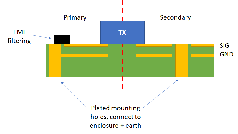
d) Use fastening screws to make it tightly combined with the shielding cavity, and the spacing of the fastening screws is less than λ/20 (depending on the specific situation).
(2) Grouping and grounding According to the structural distribution of the circuit and the size of the current, the entire circuit is divided into several relatively independent groups. Each group of circuits is grounded nearby to form a loop. The direction of the high-frequency filter capacitor in each group should be adjusted to reduce the power supply loop. Note that the grounding wire should be short and straight, and cross-overlapping is prohibited to reduce the interference caused by the common ground impedance.
(3) Grounding of RF Devices When surface mounted RF devices and filter capacitors need to be grounded, in order to reduce the grounding inductance of the device, the following requirements are required:
a) At least 2 wires should be connected to the grounding copper foil;
b) At least 2 metalized vias should be used to ground the device pins.
c) Increase the via diameter and connect several vias in parallel.
d) The bottom of some components is a grounded metal shell. Some grounding holes should be added in the projection area of the component, and the surface layer should not be wired.
(4) Correctly choose single-point grounding and multi-point grounding In low-frequency circuits, the operating frequency of the signal is less than 1MHz, and its wiring and the inductance between the devices have little effect, while the loop current formed by the grounding circuit has a greater impact on interference, so a single-point grounding should be used.
When the signal operating frequency is greater than 10MHz, the ground line impedance becomes very large. At this time, the ground line impedance should be reduced as much as possible, and multi-point grounding should be used nearby.
When the operating frequency is between 1 and 10 MHz, if one-point grounding is used, the length of the ground wire should not exceed 1/20 of the wavelength, otherwise a multi-point grounding method should be used.
(5) Separate digital circuits from analog circuits. There are both high-speed logic circuits and linear circuits on the circuit board. They should be separated as much as possible, and the ground wires of the two should not be mixed.
They should be connected to the ground wires of the power supply end respectively. The grounding area of the linear circuit should be increased as much as possible.
(6) Thicken the ground wire as much as possible. If the ground wire is very thin, the ground potential will change with the change of current, causing the timing signal level of the electronic equipment to be unstable and the anti-noise performance to deteriorate. Therefore, the ground wire should be as thick as possible so that it can pass the allowable current of the three-point printed circuit board. If possible, the width of the ground wire should be greater than 3mm.
(7) Make the ground wire a closed loop. When designing a ground wire system of a printed circuit board composed only of digital circuits, making the ground wire into a closed loop can significantly improve the anti-noise ability. The reason is that there are many integrated circuit components on the printed circuit board, especially when there are components that consume a lot of power. Due to the limitation of the thickness of the grounding wire, a large potential difference will be generated on the ground junction, causing the anti-noise ability to decrease. If the grounding structure is formed into a loop, the potential difference will be reduced and the anti-noise ability of the electronic equipment will be improved.
(8) Grounding of microstrip circuits The diameter of the single grounding hole at the terminal of the microstrip printed circuit must be larger than the width of the microstrip line, or the terminal should be grounded by a large number of small holes in a row.
(9) Grounding process requirements
a) If the process allows, the distance between the pad and the via can be shortened;
b) If the process allows, the large grounding pad can be directly covered on at least 6 grounding vias (the specific number varies depending on the size of the pad);
c) When the grounding wire needs to go a certain distance, the routing length should be shortened and must not exceed λ/20 to prevent the antenna effect from causing signal radiation;
d) Except for special purposes, there must be no isolated copper foil, and ground vias must be added to the copper foil;
e) It is forbidden to extend the terminal open-circuit wire ends on the ground copper foil.
3.Device layout
In the process of PCB design, from the perspective of EMC, the first three main factors to be considered are: the number of input/output pins, device density and power consumption. A practical rule is that the area occupied by sheet components is 20% of the substrate, and the power dissipation per square inch is not more than 2W.
In terms of device layout, in principle, related devices should be placed as close as possible, digital circuits, analog circuits and power circuits should be placed separately, and high-frequency circuits should be separated from low-frequency circuits. Devices that are prone to noise, small current circuits, high current circuits, etc. should be kept as far away from logic circuits as possible. Main interference and radiation sources such as clock circuits and high-frequency circuits should be arranged separately and away from sensitive circuits. Input and output chips should be located close to the I/O exit of the hybrid circuit package.
The connection lines of high-frequency components should be shortened as much as possible to reduce distributed parameters and mutual electromagnetic interference. Components that are susceptible to interference should not be too close to each other, and input and output should be kept as far away as possible. The oscillator should be as close as possible to the location where the clock chip is used, and away from signal interfaces and low-level signal chips. The components should be parallel or perpendicular to one side of the substrate, and the components should be arranged in parallel as much as possible. This will not only reduce the distributed parameters between components, but also conform to the manufacturing process of the hybrid circuit and be easy to produce.
The lead-out pads for power and ground on the hybrid circuit substrate should be arranged symmetrically, and it is best to evenly distribute many power and ground I/O connections. The mounting area of the bare chip is connected to the most negative potential plane.
When selecting a multilayer hybrid circuit, the interlayer arrangement of the circuit board changes with the specific circuit, but generally has the following characteristics.
(1) The power supply and ground layers are allocated in the inner layer, which can be regarded as a shielding layer, which can effectively suppress the common-mode RF interference inherent in the circuit board and reduce the distributed impedance of the high-frequency power supply.
(2) The power plane and the ground plane in the board are as close to each other as possible. Generally, the ground plane is above the power plane. In this way, the interlayer capacitance can be used as a smoothing capacitor for the power supply. At the same time, the ground plane plays a shielding role for the radiation current distributed on the power plane.
(3) The wiring layer should be arranged as close to the power supply or ground plane as possible to produce a flux cancellation effect.
In circuit design, people often only focus on improving the wiring density or pursuing uniform layout, ignoring the impact of line layout on preventing interference, causing a large number of signals to radiate into space to form interference, which may cause more electromagnetic compatibility problems. Therefore, good wiring is the key to determining the success of the design.
4.GND routing
The ground wire is not only the potential reference point for the circuit operation, but also a low-impedance loop for the signal. The most common interference on the ground wire is the ground loop interference caused by the ground loop current. Solving this type of interference problem is equivalent to solving most of the electromagnetic compatibility problems. The noise on the ground line mainly affects the ground level of the digital circuit, and when the digital circuit outputs a low level, it is more sensitive to the noise of the ground line. The interference on the ground line may not only cause the circuit to malfunction, but also cause conduction and radiation emissions. Therefore, the key to reducing these interferences is to reduce the impedance of the ground line as much as possible (for digital circuits, reducing the ground line inductance is particularly important).
Pay attention to the following points when laying out the ground line:
(1) According to different power supply voltages, the digital circuit and the analog circuit are set up with ground lines separately.
(2) The common ground line should be as thick as possible. When using a multi-layer thick film process, a special ground line surface can be set up, which helps to reduce the loop area and also reduces the efficiency of the receiving antenna. It can also serve as a shield for the signal line.
(3) Comb-shaped ground lines should be avoided. This structure makes the signal return loop very large, which will increase radiation and sensitivity, and the common impedance between chips may also cause circuit malfunction.
(4) When multiple chips are mounted on the board, a large potential difference will appear on the ground line. The ground line should be designed as a closed loop to improve the noise tolerance of the circuit.
(5) For circuit boards with both analog and digital functions, the analog ground and digital ground are usually separated and only connected at the power supply.
5.Power line routing
Generally speaking, in addition to interference caused directly by electromagnetic radiation, electromagnetic interference caused by the power line is the most common. Therefore, the layout of the power line is also very important, and the following rules should usually be followed.
(1) The power line should be as close to the ground line as possible to reduce the power supply loop area, reduce differential mode radiation, and help reduce circuit interference. The power supply loops of different power supplies should not overlap with each other.
(2) When using multi-layer technology, separate the analog power supply and the digital power supply to avoid mutual interference. Do not overlap the digital power supply with the analog power supply, otherwise coupling capacitance will be generated, destroying the separation.
(3) The power plane and the ground plane can be completely isolated by dielectric. When the frequency and speed are very high, a dielectric slurry with a low dielectric constant should be used. The power plane should be close to the ground plane and arranged below the ground plane to shield the radiation current distributed on the power plane.
(4) The power pin and ground pin of the chip should be decoupled. The decoupling capacitor uses a 0.01uF chip capacitor and should be installed close to the chip to minimize the loop area of the decoupling capacitor.
(5) When using a surface-mount chip, try to use a chip with a power pin and a ground pin close to each other, which can further reduce the power supply loop area of the decoupling capacitor and help achieve electromagnetic compatibility.
6 Signal line routing
When using a single-layer film process, a simple and applicable method is to first lay out the ground line, then arrange the key signals, such as high-speed clock signals or sensitive circuits close to their ground loops, and finally route other circuits. The signal line should be arranged according to the order of signal flow to make the signal flow on the circuit board smooth.
If you want to minimize EMI, keep the signal line as close as possible to the return signal line it forms, and make the loop area as small as possible to avoid radiation interference. Low-level signal channels cannot be close to high-level signal channels and unfiltered power lines.
Noise-sensitive wiring should not be parallel to high-current and high-speed switching lines. If possible, arrange all key wiring into strip lines. Incompatible signal lines (digital and analog, high speed and low speed, high current and low current, high voltage and low voltage, etc.) should be kept away from each other and not run in parallel. Crosstalk between signals is extremely sensitive to the length and spacing of adjacent parallel lines, so try to increase the spacing between high-speed signal lines and other parallel signal lines and reduce the parallel length.
The inductance of the conductive strip is proportional to its length and the logarithm of its length, and inversely proportional to the logarithm of its width. Therefore, the conductive strip should be as short as possible, and the length of each address line or data line of the same component should be kept consistent as much as possible. The wires used as circuit input and output should be avoided from being adjacent and parallel.
It is best to add a ground wire between them to effectively suppress crosstalk. The wiring density of low-speed signals can be relatively large, and the wiring density of high-speed signals should be as small as possible.
In the multi-layer thick film process, in addition to complying with the rules of single-layer wiring, attention should also be paid to:
Try to design a separate ground plane, and arrange the signal layer adjacent to the ground layer. When it cannot be used, a ground wire must be set near the high-frequency or sensitive circuit. The signal lines distributed on different layers should be perpendicular to each other, so as to reduce the electric and magnetic field coupling interference between the lines; the signal lines on the same layer should maintain a certain distance, and it is best to isolate them with the corresponding ground line loop to reduce the signal crosstalk between the lines. Each high-speed signal line should be limited to the same layer
The signal line should not be too close to the edge of the substrate, otherwise it will cause the characteristic impedance to change, and it is easy to generate a fringe field and increase the outward radiation.
7.Clock line wiring
The clock circuit occupies an important position in the digital circuit, and it is also the main source of electromagnetic radiation. The spectrum of the radiation energy of a clock signal with a 2ns rising edge can reach 160MHz. Therefore, designing a good clock circuit is the key to ensuring the electromagnetic compatibility of the entire circuit. Regarding the layout of the clock circuit, there are the following points to note:
(1) Do not use a daisy chain structure to transmit the clock signal, but a star structure, that is, all clock loads are directly connected to the clock power driver.
(2) All conductors connected to the input/output of the crystal oscillator should be as short as possible to reduce noise interference and the influence of distributed capacitance on the crystal oscillator.
(3) The ground wire of the crystal oscillator capacitor should be connected to the device using a conductor that is as wide and short as possible; the digital ground pin closest to the crystal oscillator should have as few vias as possible.
8.Shielding
(1) RF signals can radiate in the air medium. The greater the spatial distance and the lower the operating frequency, the smaller the parasitic coupling at the input and output ends, and the greater the isolation. The typical spatial isolation of PCB is about 50dB.
(2) Sensitive circuits and strong radiation source circuits should be shielded, but if the design and processing are difficult (such as space or cost restrictions, etc.), it can be omitted, but the final decision must be made after testing. These circuits are:
a) The front end of the receiving circuit is a sensitive circuit with a very small signal, so shielding should be used.
b) The RF unit and the IF unit must be shielded. The IF signal of the receiving channel will cause great interference to the RF signal. Conversely, the RF signal of the transmitting channel will also cause radiation interference to the IF signal.
c) Oscillation circuit: a strong radiation source. The local oscillator source must be shielded separately. Due to the high level of the local oscillator, it will cause great radiation interference to other units.
d) Power amplifier and antenna feed circuit: a strong radiation source. The signal is very strong and needs to be shielded.
e) Digital signal processing circuit: a strong radiation source. The steep upper and lower edges of high-speed digital signals will interfere with the analog RF signal.
f) Cascade amplifier circuit: the total gain may exceed the spatial isolation from the output to the input end, which satisfies one of the oscillation conditions and the circuit may self-excite. If the same-frequency gain of the circuit in the cavity exceeds 30-50dB, a metal shielding plate must be welded or installed on the PCB board to increase the isolation. In actual design, the frequency, power, and gain should be comprehensively considered to decide whether to add a shielding plate.
g) Cascaded filtering, switching, and attenuation circuits: In the same shielding cavity, the out-of-band attenuation of the cascaded filtering circuit, the isolation of the cascaded switching circuit, and the attenuation of the cascaded attenuation circuit must be less than 30-50dB. If this value is exceeded, a metal shielding plate must be welded or installed on the PCB board to increase the isolation. In actual design, the frequency, power, and gain should be considered comprehensively to decide whether to add a shielding plate.
h) When the transceiver unit is mixed, it should be shielded.
i) When the digital and analog are mixed, the clock line should be wrapped with copper foil for isolation or shielding.


