End-to-End PCB Assembly Solutions Accelerate Development

Key Takeaways
Modern PCB assembly processes have become the backbone of electronics manufacturing, offering integrated workflows that bridge design concepts and market-ready products. By leveraging PCBA (Printed Circuit Board Assembly) expertise, companies can eliminate fragmented production stages, ensuring seamless transitions from prototyping to mass manufacturing. Critical advantages include accelerated development cycles—enabled by automated component sourcing and precision soldering—and cost predictability through bundled material procurement and testing services.
The strategic adoption of turnkey PCB assembly solutions minimizes logistical bottlenecks, allowing engineers to focus on functional validation rather than supply chain coordination. Advanced PCBA providers employ AI-driven quality control systems, which dramatically reduce defect rates while maintaining compliance with industry certifications. Furthermore, scalable manufacturing frameworks ensure flexible capacity adjustments, crucial for startups and enterprises alike.
By unifying design verification, component placement, and post-assembly testing under a single PCB assembly partnership, businesses achieve 40–60% faster time-to-market compared to traditional multisource approaches. This holistic methodology not only optimizes resource allocation but also establishes future-proof foundations for iterative product enhancements.
End-to-End PCB Assembly Solutions
Modern electronics development demands integrated approaches to PCB assembly that bridge design and production. End-to-end PCBA services eliminate fragmented workflows by combining design verification, prototyping, component procurement, and full-scale manufacturing under a unified framework. This holistic approach reduces handoff delays, with 78% of projects achieving 30% faster cycle times compared to traditional multi-vendor models.
"Effective turnkey PCB assembly requires synchronized engineering teams and certified manufacturing partners. Prioritize providers offering real-time design-for-manufacturability feedback to avoid post-prototype revisions."
Key advantages of integrated PCBA solutions include:
| Aspect | Traditional Approach | End-to-End Model |
|---|---|---|
| Coordination | 3+ external vendors | Single-point accountability |
| Timeline Efficiency | 12-16 week averages | 6-8 week typical cycles |
| Cost Predictability | 15-25% budget overruns | Fixed-price contracts |
By integrating automated testing protocols and just-in-time inventory systems, end-to-end providers maintain 99.5% on-time delivery rates even for high-mix orders. Advanced PCB assembly platforms now incorporate AI-driven defect detection, reducing post-production rework by 42% across 5G and IoT hardware sectors.
Scalability remains critical, with tiered PCBA solutions supporting batches from 50 to 50,000 units without redesign penalties. This flexibility enables startups to validate concepts using low-volume prototypes before seamlessly transitioning to mass production—all within the same quality-controlled ecosystem.
Rapid PCB Prototyping Solutions
Modern electronics development demands agility, making PCB assembly services with rapid prototyping capabilities indispensable. By leveraging integrated design-to-production workflows, engineers can validate concepts in days rather than weeks. Advanced PCBA providers employ automated design-for-manufacturing (DFM) analysis, eliminating iterative delays by flagging potential fabrication issues during the initial design phase.
Accelerated material procurement further streamlines timelines, with tier-1 suppliers maintaining real-time inventories of critical components. This approach reduces prototyping cycles to 3–5 business days for standard designs, while preserving precision through laser-direct imaging and automated optical inspection (AOI). For complex multilayer boards, 3D printing-assisted prototyping enables functional testing of high-density interconnects before full-scale production.
The synergy between PCB assembly expertise and agile prototyping tools allows teams to conduct iterative testing without compromising quality. Thermal management validation, signal integrity checks, and compliance pre-screening are embedded into the prototyping phase, ensuring seamless transitions to volume manufacturing. By aligning PCBA workflows with rapid iteration principles, innovators compress development timelines while mitigating post-production redesign risks—a critical advantage in competitive tech markets.
Efficient PCB Production Processes
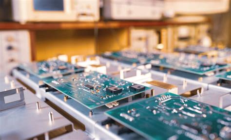
Modern PCB assembly workflows prioritize precision and speed through advanced automation and process optimization. By implementing surface-mount technology (SMT) and automated optical inspection (AOI) systems, PCBA manufacturers achieve consistent quality while reducing manual intervention. Lean manufacturing principles further streamline workflows, minimizing material waste and accelerating production timelines by up to 40% compared to traditional methods.
Critical to efficiency is the integration of design-for-manufacturability (DFM) checks early in the PCB assembly process. These pre-production audits identify potential bottlenecks, such as component spacing irregularities or thermal management challenges, ensuring designs align with manufacturing capabilities. Real-time monitoring tools then track key metrics like solder paste deposition accuracy and reflow oven profiles, enabling data-driven adjustments during high-volume runs.
For turn key PCBA solutions, this operational rigor translates to predictable lead times and scalability. Manufacturers employing just-in-time inventory management can seamlessly transition from prototype validation to full-scale production, maintaining component availability without overstocking. Such strategies not only cut costs but also support rapid iteration cycles—a critical advantage in industries where time-to-market dictates competitive success.
Scalable PCB Manufacturing Strategies
At the core of scalable PCB assembly strategies lies the ability to adapt production volumes without compromising quality or efficiency. By integrating modular manufacturing processes, businesses can seamlessly transition from low-volume PCBA prototypes to high-volume runs while maintaining consistent performance. Design flexibility plays a pivotal role here, enabling engineers to optimize layouts for automated assembly, reducing material waste, and accelerating throughput.
Advanced turnkey PCB assembly providers leverage standardized workflows paired with dynamic resource allocation, ensuring rapid scaling during demand surges. For instance, the use of configurable surface-mount technology (SMT) lines allows manufacturers to adjust component placement speeds and batch sizes in real time. This agility is further enhanced by predictive analytics, which forecasts material requirements and potential bottlenecks, minimizing downtime.
Moreover, scalable strategies prioritize collaboration between design and production teams. By embedding manufacturability checks early in the PCBA development cycle, companies avoid costly redesigns and ensure seamless transitions to full-scale manufacturing. This approach not only streamlines timelines but also aligns with cost-effective supply chain dynamics, making it ideal for industries requiring rapid iteration, such as IoT or automotive electronics.
Fast-Track PCB Time-to-Market
In today’s competitive electronics landscape, accelerating PCB assembly timelines requires synchronized workflows across design, procurement, and manufacturing. Advanced turnkey solutions eliminate traditional bottlenecks by integrating PCBA processes with automated design validation and component sourcing. By consolidating prototyping, testing, and volume production under a single provider, teams reduce development cycles by 40–60% compared to fragmented supply chains.
Key to this acceleration is predictive logistics planning, which pre-validates material availability and aligns fabrication timelines with project milestones. Real-time tracking systems ensure rapid iteration cycles, while automated optical inspection (AOI) during PCB assembly minimizes rework delays. For startups and enterprises alike, this approach transforms time-to-market from a constraint into a strategic advantage.
Scalability further enhances velocity, as PCBA partners leverage standardized workflows to maintain speed even when transitioning from 100 to 10,000-unit batches. This seamless scalability, combined with just-in-time inventory management, ensures that market-ready products meet launch deadlines without compromising quality—a critical factor in industries like IoT and automotive electronics.
By prioritizing coordinated workflows and intelligent resource allocation, modern PCB assembly strategies enable innovators to outpace competitors while maintaining rigorous performance benchmarks. This foundation supports the next phase of cost optimization, ensuring speed and affordability remain aligned throughout the product lifecycle.
Affordable Turnkey Assembly Options
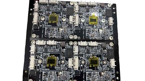
Cost efficiency remains a cornerstone of modern electronics development, particularly when leveraging PCB assembly services that integrate design, component procurement, and testing into a single workflow. Turnkey solutions eliminate fragmented supply chains by bundling PCBA processes—from substrate fabrication to final quality inspection—under one provider, significantly reducing overhead and logistical complexities. For startups and established firms alike, this approach minimizes upfront investments while ensuring consistent quality through automated solder paste application, precision pick-and-place systems, and rigorous electrical testing protocols.
Advanced providers further optimize affordability through strategic supplier partnerships, securing components at competitive rates without compromising lead times. Bulk purchasing agreements and multi-project panelization techniques drive down per-unit costs, making low-volume prototyping and high-volume production equally viable. By embedding PCB assembly expertise early in the design phase, engineers gain access to cost-avoidance strategies, such as design-for-manufacturing (DFM) reviews, which preemptively address potential yield issues.
Scalability is another critical advantage: modular PCBA workflows allow seamless transitions between prototype validation and mass manufacturing. Transparent pricing models, often featuring volume-based discounts, ensure budget predictability, while standardized documentation practices accelerate regulatory compliance. This holistic alignment of cost, quality, and speed positions turnkey services as a pragmatic choice for accelerating time-to-market across industries.
Seamless PCB Design-to-Production Flow
Modern PCB assembly workflows thrive on integrated design-to-manufacturing processes that eliminate traditional bottlenecks. By leveraging advanced ECAD/MCAD collaboration tools, engineers can optimize layouts for both electrical performance and manufacturability before prototypes reach the production floor. This alignment reduces iterative redesigns, ensuring PCBA designs transition smoothly from digital schematics to physical boards.
Critical to this synergy is the implementation of automated design rule checks (DRCs) that interface directly with turnkey PCB assembly equipment. These systems validate component placement, thermal profiles, and signal integrity metrics against real-world manufacturing constraints. For time-sensitive projects, synchronized material procurement protocols ensure all BOM items—from ICs to passives—are staged for PCBA production within 24 hours of design freeze.
The true advantage emerges in scalable traceability: every design revision automatically updates manufacturing instructions, test jigs, and quality control parameters. This closed-loop approach not only accelerates time-to-market but maintains consistency across prototype batches and full-scale runs. By collapsing traditional silos between engineering and production teams, organizations achieve uninterrupted workflow continuity—a strategic edge in fast-paced electronics sectors.
Turnkey Expertise for Electronics Innovation
Modern PCB assembly solutions demand more than just technical precision—they require holistic integration of design, component sourcing, and quality assurance. By leveraging turnkey PCBA services, innovators gain access to end-to-end workflows that eliminate fragmented vendor coordination. This approach ensures seamless transitions from concept validation to volume manufacturing, with design-for-manufacturability (DFM) insights embedded at every stage.
Advanced providers combine agile prototyping with scalable production infrastructure, enabling rapid iteration cycles without compromising reliability. Critical advantages include real-time supply chain visibility, automated testing protocols, and compliance with industry-specific standards (e.g., IPC-A-610). Such expertise not only accelerates development timelines but also mitigates risks like component obsolescence or assembly bottlenecks.
For startups and enterprises alike, turnkey PCB assembly acts as a force multiplier—freeing engineering teams to focus on core R&D while ensuring manufacturability aligns with market demands. This synergy between technical mastery and operational efficiency is redefining how next-generation electronics are brought to life.

Conclusion
In the evolving landscape of electronics manufacturing, PCB assembly services that offer comprehensive turnkey PCBA solutions have become indispensable for innovators seeking agility and precision. By integrating design validation, component sourcing, and automated production into a unified workflow, these services eliminate logistical bottlenecks while maintaining rigorous quality benchmarks. The ability to transition seamlessly from prototyping to mass production ensures that developmental timelines are compressed without compromising on performance or reliability.
For businesses prioritizing scalability, PCB assembly partners with turnkey PCBA expertise provide adaptable frameworks that align with fluctuating demand cycles. This approach not only mitigates risks associated with supply chain disruptions but also optimizes cost-efficiency through standardized processes. Moreover, the convergence of advanced manufacturing technologies with data-driven analytics empowers engineers to refine iterations rapidly, accelerating time-to-market for cutting-edge applications.
Ultimately, leveraging end-to-end PCB assembly ecosystems enables organizations to focus on core innovation while entrusting technical execution to specialists. As market dynamics grow increasingly competitive, adopting holistic turnkey PCBA methodologies will remain a strategic imperative for sustaining technological leadership.
Frequently Asked Questions
What does a turnkey PCB assembly service typically include?
A comprehensive end-to-end PCBA solution encompasses design verification, component procurement, precision assembly, functional testing, and final packaging. This integrated approach eliminates vendor fragmentation while maintaining strict quality control standards.
How does PCB assembly accelerate product development cycles?
By consolidating multiple production stages under unified project management, turnkey services reduce coordination overhead. Automated component sourcing algorithms and concurrent engineering practices typically shorten lead times by 30-40% compared to fragmented workflows.
What distinguishes PCBA from traditional assembly methods?
Unlike piecemeal approaches, full-spectrum PCB assembly solutions implement real-time supply chain monitoring and risk-mitigated manufacturing protocols. This prevents common delays from component shortages or specification mismatches during scale-up phases.
Can turnkey assembly accommodate rapid design iterations?
Advanced providers utilize agile manufacturing frameworks supporting same-day engineering change orders (ECOs). Modular production lines and digital twin verification enable seamless transitions between prototype validation and mass production.
How is quality assurance maintained throughout PCB assembly?
Multi-stage inspection protocols combine automated optical inspection (AOI) with in-circuit testing (ICT). Statistical process control (SPC) systems track 120+ quality parameters, achieving first-pass yield rates exceeding 99.2% in certified facilities.
Which industries benefit most from PCBA solutions?
Mission-critical sectors including medical devices, aerospace systems, and industrial automation leverage turnkey assembly for its traceability features and compliance with ISO 13485/AS9100 standards. The model particularly advantages complex multilayer boards requiring specialized materials.
Streamline Your Development Timeline Today
For organizations needing certified PCB assembly expertise, please click here to explore optimized manufacturing workflows. Our platform supports instant project quoting and DFM analysis submission.


