Environmentally Friendly PCB Materials: A Sustainable Approach to Electronics Manufacturing
Introduction
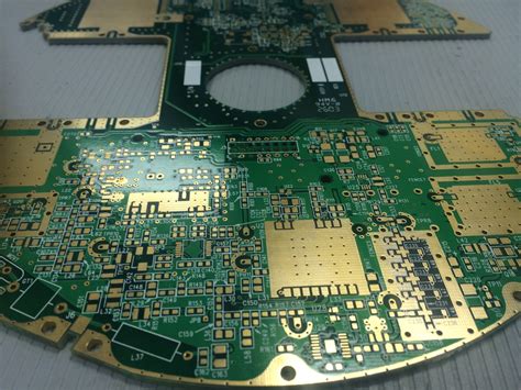
The electronics industry has experienced exponential growth over the past few decades, leading to increased demand for printed circuit boards (PCBs). However, traditional PCB manufacturing relies on hazardous materials, including lead-based solders, brominated flame retardants (BFRs), and non-biodegradable substrates, contributing to environmental pollution and health risks.
As sustainability becomes a global priority, the development and adoption of environmentally friendly PCB materials are critical. These materials aim to reduce toxic waste, improve recyclability, and lower carbon footprints while maintaining performance. This article explores sustainable alternatives in PCB manufacturing, including biodegradable substrates, halogen-free laminates, lead-free solders, and innovative recycling methods.
1. The Environmental Impact of Conventional PCBs
Traditional PCBs contain several harmful components:
- Flame Retardants (BFRs & CFRs): Brominated and chlorinated flame retardants release toxic dioxins when incinerated.
- Lead-Based Solders: Lead is a neurotoxin that contaminates soil and water.
- Non-Recyclable Substrates: Fiberglass-reinforced epoxy (FR-4) is durable but difficult to recycle.
- Chemical Etching Processes: Use of acids and heavy metals generates hazardous waste.
These materials contribute to electronic waste (e-waste), which accounts for 53.6 million metric tons annually (Global E-waste Monitor 2023). Sustainable alternatives are necessary to mitigate these environmental hazards.
2. Eco-Friendly PCB Substrates
a) Biodegradable and Bio-Based Materials
Researchers are developing PCB substrates from renewable sources:
- Polylactic Acid (PLA): A biodegradable polymer derived from corn starch or sugarcane.
- Cellulose-Based Composites: Natural fibers combined with resins for improved biodegradability.
- Mycelium (Mushroom-Based Boards): Fungi-grown substrates that decompose naturally.
Challenges: Lower thermal resistance and mechanical strength compared to FR-4. However, hybrid composites are being tested to enhance durability.
b) Halogen-Free Laminates
Halogen-free materials eliminate bromine and chlorine, reducing toxic emissions:
- Phosphorus-Based Flame Retardants: Less harmful than BFRs.
- Polyimide and PTFE Alternatives: High-performance, recyclable options.
Companies like Rogers Corporation and Isola Group offer halogen-free laminates for high-frequency applications.
3. Lead-Free Soldering
The Restriction of Hazardous Substances (RoHS) Directive banned lead in electronics, leading to alternatives:
- Tin-Silver-Copper (SAC) Alloys: Most common replacement (e.g., SAC305: 96.5% Sn, 3% Ag, 0.5% Cu).
- Bismuth-Based Solders: Lower melting point, suitable for heat-sensitive components.
- Zinc-Aluminum Alloys: Emerging as a low-cost, eco-friendly option.
Challenges: Higher melting points require modified reflow processes, and some alloys are more brittle.
4. Sustainable Manufacturing Processes
a) Dry Film Photoresists
Traditional liquid photoresists use harmful solvents. Dry film alternatives reduce chemical waste.
b) Additive Manufacturing (3D Printing)
- Inkjet Printing of Conductive Traces: Reduces material waste by depositing only required amounts.
- Aerosol Jet Printing: Enables fine-patterning without etching chemicals.
c) Chemical-Free Etching
- Mechanical Milling: CNC-based etching eliminates acid use.
- Laser Direct Structuring (LDS): Lasers create circuit patterns without chemicals.
5. Recycling and Circular Economy
a) PCB Decomposition Techniques
- Bioleaching: Using bacteria to extract metals (e.g., copper, gold) from waste PCBs.
- Hydrothermal Processing: High-pressure water dissolves adhesives for easier separation.
b) Upcycling E-Waste
- Recovered Metals: Gold, silver, and copper can be reused in new PCBs.
- Reclaimed Resins: Crushed PCB waste can be repurposed in construction materials.
Companies like Apple and Dell have implemented PCB recycling programs to recover valuable materials.

6. Case Studies & Industry Adoption
- Google’s Circular PCB Initiative: Partnering with suppliers to use recycled materials in server PCBs.
- Samsung’s Eco-Packaging: Using PCB waste fibers for sustainable packaging.
- European Union’s Green Deal: Funding research into bio-based electronics.
7. Future Trends
- Self-Healing PCBs: Materials that repair cracks, extending product lifespan.
- Nanocellulose Substrates: Ultra-thin, biodegradable, and high-strength alternatives.
- AI-Driven Material Discovery: Machine learning accelerates the development of green composites.
Conclusion
The shift toward environmentally friendly PCB materials is essential for reducing e-waste, minimizing toxic exposure, and promoting a circular economy. While challenges remain in performance and cost, advancements in biodegradable substrates, lead-free solders, and sustainable manufacturing are paving the way for greener electronics.
Industry collaboration, stricter regulations (e.g., RoHS, REACH), and consumer demand for sustainable products will drive further innovation. By adopting these solutions, manufacturers can align with global sustainability goals while maintaining technological progress.


