ESA-Certified PCB Manufacturers: Space-Grade Compliance
Key Takeaways
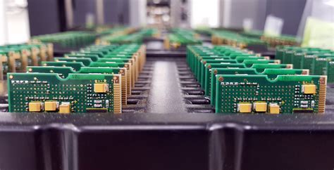
When evaluating PCB manufacturing partners for space applications, you need to verify compliance with ECSS-Q-ST-70-60C—the gold standard for ESA-certified electronics. This involves rigorous material selection, precision in microvia-driven HDI technology, and adherence to thermal cycling tests that simulate orbital conditions. Leading PCB manufacturing companies like Italy’s Cistelaier demonstrate how specialized processes, such as laser-drilled microvias below 100μm, ensure reliability in extreme environments.
Understanding PCB manufacturing cost factors is critical: space-grade boards require high-Dk laminates, embedded passives, and 20+ layer stacks, which escalate expenses but eliminate long-term failure risks. ESA engineer Stan Heltzel emphasizes that quality protocols—from ionic contamination controls to cross-sectional analysis—are non-negotiable. For PCB manufacturing business leaders, aligning with ESA standards opens doors to satellite and rover projects, though it demands investments in cleanrooms and ECSS-compliant documentation systems.
To streamline compliance, review the ESA’s technical requirements for traceability and defect rates. Transitioning from commercial to space-ready production requires balancing innovation with audited processes—a challenge where ESA-qualified partners excel.

ESA Certification: ECSS-Q-ST-70-60C Standards
When evaluating PCB manufacturing companies for space applications, compliance with ESA’s ECSS-Q-ST-70-60C standards is non-negotiable. These rigorous protocols govern everything from material selection to final testing, ensuring reliability in extreme environments like radiation exposure and thermal vacuum conditions. For manufacturers, achieving ESA certification involves stringent audits of PCB manufacturing processes, including microvia reliability, solder mask adhesion, and copper plating uniformity.
A key challenge lies in balancing PCB manufacturing cost with compliance demands. For instance, ESA-certified boards often require specialized substrates like polyimide or ceramic-filled laminates, which can increase material expenses by 30–50% compared to commercial-grade alternatives. Additionally, the standards mandate exhaustive testing phases—such as thermal cycling (-55°C to +125°C) and vibration simulations—that extend production timelines.
| Compliance Factor | ESA Requirement | Commercial Equivalent |
|---|---|---|
| Thermal Cycling | 1,000 cycles minimum | 100–300 cycles |
| Microvia Aspect Ratio | ≤ 1:1 | ≤ 1:1.5 |
| Outgassing (TML/CVCM) | ≤ 1.0% / ≤ 0.1% | Not regulated |
To sustain a competitive PCB manufacturing business, companies must integrate these standards into their workflows without compromising scalability. This often involves adopting advanced HDI techniques and automated inspection systems to maintain yield rates. By aligning with ECSS-Q-ST-70-60C, manufacturers not only meet ESA’s criteria but also position themselves as leaders in high-reliability aerospace solutions.
Cistelaier: Italy’s ESA-Qualified PCB Pioneer
When navigating the complex landscape of PCB manufacturing companies for space applications, you’ll find Cistelaier standing out as Italy’s first ESA-qualified partner. Specializing in high-density interconnect (HDI) designs, their PCB manufacturing processes adhere strictly to ECSS-Q-ST-70-60C standards, ensuring reliability in extreme orbital conditions. What sets them apart is their proprietary microvia-driven HDI technology, which enables circuitry to withstand thermal cycling and radiation exposure—critical for satellite systems.
Tip: Always verify if your chosen PCB manufacturing business holds certifications for traceability and material trace testing, as these are non-negotiable for ESA compliance.
While PCB manufacturing cost often rises with aerospace-grade requirements, Cistelaier optimizes material selection and layer stacking to balance performance and budget. Their expertise in laser drilling and sequential lamination minimizes signal loss, even in multi-layered designs. For businesses prioritizing longevity, their conformal coating techniques add an extra layer of protection against moisture and contaminants.
By integrating ESA’s quality protocols into every production phase, this Italian innovator demonstrates how specialized PCB manufacturing can meet both technical and regulatory demands without compromising scalability.
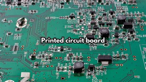
Microvia Technology in Space-Grade HDI PCBs
When selecting PCB manufacturing companies for space applications, understanding the role of microvia technology in high-density interconnect (HDI) designs becomes critical. These laser-drilled microvias—typically under 150 microns in diameter—enable precise electrical connections across multilayer boards while minimizing signal loss, a non-negotiable requirement under ESA’s ECSS-Q-ST-70-60C standards. For PCB manufacturing businesses specializing in satellite or spacecraft systems, this technology ensures compliance with strict thermal cycling and vibration resistance protocols.
Advanced PCB manufacturing processes leverage microvias to achieve stacked via configurations and blind/buried via structures, reducing layer count without compromising reliability. This precision directly impacts PCB manufacturing cost, as tighter tolerances demand specialized laser systems and rigorous testing. However, the trade-off delivers unparalleled performance in extreme environments, from radiation-heavy orbits to rapid temperature fluctuations. Leading ESA-qualified suppliers combine microvia-driven HDI with low-loss dielectrics and controlled impedance routing to meet mission-critical signal integrity demands.
As you evaluate suppliers, prioritize firms with documented expertise in scaling microvia technology for space-grade applications—proof they’ve mastered the balance between miniaturization and durability required for orbital hardware.
ESA Engineer Insights: PCB Quality Protocols
When navigating PCB manufacturing for space applications, you’ll find that ESA-certified providers adhere to rigorous quality protocols rooted in ECSS-Q-ST-70-60C standards. These protocols demand microscopic precision in material selection, layer alignment, and thermal management—non-negotiables for circuitry operating in extreme environments. For PCB manufacturing companies, this translates to specialized processes like laser-drilled microvias and controlled impedance testing, which ensure signal integrity across satellite systems.
A key challenge lies in balancing PCB manufacturing cost with compliance. ESA engineers, including veteran Stan Heltzel, emphasize traceability frameworks that document every production stage—from laminate procurement to final inspection. This level of accountability minimizes defects but requires investments in advanced equipment and staff training, factors that influence pricing models for PCB manufacturing business operations.
You’ll notice that ESA-approved workflows prioritize failure mode analysis over speed, often extending lead times by 20–30% compared to commercial-grade production. However, this meticulous approach safeguards against mission-critical failures, aligning with Heltzel’s philosophy: “In space, quality isn’t a metric—it’s the foundation.” By integrating these protocols, manufacturers meet not just ESA’s technical benchmarks but also the reliability expectations of aerospace stakeholders.
ECSS Compliance for Satellite-Ready Circuitry
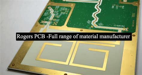
When developing PCB manufacturing processes for space applications, adherence to the ECSS-Q-ST-70-60C standard becomes non-negotiable. This framework mandates rigorous controls over material selection, traceability, and thermal performance to ensure circuits withstand extreme radiation, vacuum, and vibration. For PCB manufacturing companies, achieving compliance requires balancing advanced fabrication techniques with meticulous documentation—a challenge that directly impacts PCB manufacturing cost due to specialized materials like polyimide substrates and laser-drilled microvias.
Satellite-ready designs demand zero-defect tolerance, pushing manufacturers to implement automated optical inspection (AOI) and cross-sectional analysis at every production stage. These protocols verify microvia integrity and copper plating uniformity, critical for high-density interconnects (HDIs) in compact satellite modules. However, scaling such precision across a PCB manufacturing business introduces complexities, particularly when reconciling ESA’s 14-layer maximum stackup rule with signal integrity requirements.
For example, Cistelaier’s approach combines ionized cleanliness protocols with ECSS-alented process flows, reducing particulate contamination risks during lamination. This ensures boards meet outgassing thresholds below 1% TML—a key criterion for avoiding condensate formation in low-Earth orbit. By aligning PCB manufacturing workflows with these standards, companies mitigate qualification delays while maintaining cost-efficiency for high-reliability aerospace contracts.
HDI Innovations in ESA-Certified Manufacturing
When selecting PCB manufacturing companies for space applications, you need solutions that balance cutting-edge technology with strict compliance. High-density interconnect (HDI) innovations are revolutionizing PCB manufacturing for ESA-certified projects, particularly through advanced microvia architectures. These laser-drilled microvias enable tighter trace spacing and higher layer counts—critical for satellite systems where miniaturization and reliability are non-negotiable.
Leading manufacturers integrate sequential lamination and laser direct imaging to meet ECSS-Q-ST-70-60C tolerances, ensuring signal integrity in extreme thermal-vacuum conditions. However, such precision impacts PCB manufacturing cost, as specialized materials like polyimide substrates and low-outgassing adhesives add complexity. For example, Cistelaier’s ESA-qualified HDI boards use 25µm microvias to reduce impedance fluctuations, a technique validated by ESA engineer Stan Heltzel’s quality protocols.
For your PCB manufacturing business, adopting HDI processes isn’t just about technical prowess—it’s about aligning with space-grade verification cycles. Every layer stack-up undergoes rigorous thermal cycling tests, while automated optical inspection (AOI) systems detect sub-5µm defects. This fusion of innovation and compliance ensures your designs survive launch vibrations and decades-long orbital operations without compromising performance.
Stan Heltzel’s Role in ESA PCB Qualification
When evaluating PCB manufacturing companies for space applications, understanding the role of experts like Stan Heltzel becomes critical. As a senior ESA engineer specializing in ECSS-Q-ST-70-60C compliance, Heltzel’s protocols directly influence how manufacturers address PCB manufacturing cost and technical precision. His work ensures that microvia-driven HDI technologies align with radiation-hardening requirements, a non-negotiable for satellite-ready circuitry.
Heltzel’s quality frameworks emphasize traceability across every layer of PCB manufacturing, from material selection to final inspection. For businesses in the PCB manufacturing business, his guidelines translate into rigorous documentation practices and defect-rate benchmarks—factors that determine eligibility for ESA projects. By standardizing testing parameters for thermal cycling and outgassing, he mitigates risks that could escalate PCB manufacturing cost due to post-launch failures.
His collaboration with manufacturers like Cistelaier highlights how ESA-certified processes balance innovation with reliability. For example, Heltzel’s insistence on laser-drilled microvias not only meets ESA standards but also pushes PCB manufacturing companies to adopt scalable high-density interconnect solutions. This approach ensures that compliance doesn’t stifle technological advancement—a delicate equilibrium in space-grade fabrication.
Ultimately, Heltzel’s methodologies redefine what it means to operate in the PCB manufacturing business, where adherence to ECSS protocols isn’t just about certification—it’s about survivability in extreme environments.
Meeting ESA Standards: PCB Fabrication Challenges
Achieving ESA certification demands overcoming rigorous technical hurdles in PCB manufacturing, particularly when balancing performance with the extreme reliability required for space applications. Thermal management becomes critical, as boards must withstand temperature fluctuations from -150°C to +125°C without delamination. PCB manufacturing companies face added complexity in material selection, needing ultra-low outgassing substrates to prevent contamination in vacuum environments.
The ECSS-Q-ST-70-60C standards further mandate trace spacing tolerances under 25µm, pushing PCB manufacturing business operations to adopt laser-direct imaging (LDI) systems. Even minor deviations in impedance control or via plating thickness can disqualify a batch, escalating PCB manufacturing cost by 30-50% compared to commercial-grade production. To maintain compliance, suppliers like Cistelaier implement cross-sectional microsection analysis at every stage, ensuring layer alignment stays within ±2% of design specifications.
Transitioning to ESA-grade production also requires rethinking workflows. For instance, cleanroom protocols rated ISO Class 5 or better are non-negotiable, while documentation must trace every material lot back to its origin—a stark contrast to conventional PCB manufacturing practices. These challenges underscore why fewer than 12% of global fabricators meet ESA’s benchmarks, making qualification a strategic differentiator in aerospace electronics.

Conclusion
When selecting PCB manufacturing partners for space applications, understanding certification requirements becomes critical. ESA-qualified PCB manufacturing companies demonstrate proven adherence to rigorous ECSS-Q-ST-70-60C protocols, ensuring reliability in extreme environments. While PCB manufacturing cost for space-grade projects often exceeds terrestrial applications, the investment safeguards mission-critical performance through advanced processes like microvia-driven HDI fabrication. For businesses operating in the PCB manufacturing business, balancing technical precision with cost-efficiency requires leveraging specialized expertise—such as Cistelaier’s multi-layer bonding techniques—to meet ESA’s traceability demands.
Challenges like material selection and thermal management underscore why partnering with certified manufacturers remains non-negotiable. By prioritizing ESA-compliant practices, you ensure your circuitry aligns with satellite-ready standards while mitigating risks inherent to orbital deployments. Whether scaling production or refining quality controls, aligning with certified partners bridges the gap between aerospace innovation and manufacturable solutions.
Frequently Asked Questions
What distinguishes ESA-certified PCB manufacturing from standard processes?
ESA certification requires adherence to ECSS-Q-ST-70-60C standards, which mandate rigorous testing for thermal cycling, radiation resistance, and microvia reliability. Unlike commercial PCB manufacturing companies, certified providers implement traceability systems for every layer and component.
How does PCB manufacturing cost compare for space-grade vs. consumer-grade boards?
PCB manufacturing cost increases by 40-60% for space-grade designs due to specialized materials like polyimide substrates and advanced quality controls. However, this ensures compliance with ESA’s zero-defect tolerance—critical for satellite and spacecraft longevity.
Can traditional PCB manufacturing business models adapt to ESA standards?
Transitioning requires investments in microvia-driven HDI tech and staff training on ECSS protocols. Most PCB manufacturing businesses partner with ESA-qualified labs for audits, as seen in Cistelaier’s collaboration with engineers like Stan Heltzel to refine failure analysis workflows.
Why choose ESA-certified providers for high-reliability applications?
These manufacturers guarantee lot-to-lot consistency and validate designs through thermal vacuum testing. Their expertise minimizes risks of delamination or signal loss—common pitfalls in non-compliant PCB manufacturing.
Ready to Explore ESA-Certified Solutions?
For tailored guidance on space-grade PCB manufacturing, please click here to connect with specialists. Ensure your designs meet ESA’s exacting standards with verified expertise.


