Essential Guidelines for Achieving Excellent PCB Design

Key Takeaways
Achieving excellent PCB design requires an understanding of several critical aspects that directly influence the outcome of your projects. For instance, the pcb manufacturing cost can vary significantly based on the complexity of your designs and the materials used. By adopting best practices in layout and component placement, you can not only reduce costs but also enhance the reliability of your product. Moreover, employing efficient routing techniques is crucial for avoiding common pitfalls that can complicate the pcb manufacturing business. Remember, selecting reputable pcb manufacturing companies is just as important; they should have a proven track record in delivering high-quality services that align with your design specifications.
"A successful PCB design harmonizes technical precision and efficient production logistics."
Stay mindful of how choices you make during the design phase may affect the overall performance and manufacturability of your final product. Engaging with industry standards during this process will support you in avoiding costly mistakes and ensuring a smoother transition from design to prototype, ultimately benefiting both you and your manufacturer. The focus on detail in every stage helps secure a reliable output, paving the way for innovations in future projects.
Introduction to Good PCB Design Practices
Achieving excellent PCB design is a multifaceted endeavor that requires careful consideration of several factors. As you begin your journey into the realm of PCB manufacturing, it’s crucial to establish a solid foundation in the principles and practices that govern effective layouts. To start, you must appreciate the significance of both aesthetics and functionality; good design not only looks appealing but also promotes reliable performance. You should focus on understanding how your choices affect the PCB manufacturing cost. Selecting high-quality materials and components can significantly influence both the performance of your circuit board and the overall production expenses. Partnering with reputable PCB manufacturing companies can also provide insights into cost-saving techniques without compromising quality.
Incorporating best practices from the onset sets the stage for improved efficiency in your design process. Think about factors like traces and component placement; effective routing can minimize electromagnetic interference while ensuring clear signal pathways. Moreover, it’s essential to plan for manufacturability early in your design phase to avoid costly revisions later on that can arise during production runs. Being mindful of these aspects not only strengthens your design but also contributes positively to your overall PCB manufacturing business outcomes, enhancing both market competitiveness and client satisfaction. Therefore, as you dive deeper into the technicalities of your designs, remember that these foundational practices will serve as vital pillars supporting every successful PCB project you undertake.
Key Principles for Efficient PCB Layout
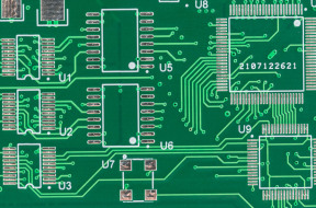
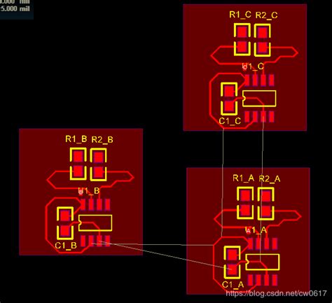
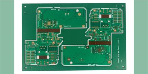
Achieving an efficient PCB layout is crucial for the overall performance and success of your project. To begin with, you should prioritize the placement of components based on their function and the paths that signals will follow. Consider grouping related components together to minimize the length of connections, which contributes to less interference and improved signal integrity. Additionally, keep in mind the PCB manufacturing cost can be significantly reduced by optimizing space and minimizing layers where possible. Ensure that trace widths are adequate for current carrying capacity while maintaining minimal lengths to enhance performance; this is especially important when working with PCB manufacturing companies that focus on high-quality outputs. Using appropriate routing techniques can also facilitate efficient designs; try to avoid sharp corners as they can create unwanted inductance and reduce reliability. Moreover, you should consistently check your design against standard specifications to avoid common pitfalls in PCB manufacturing processes. This diligence is essential not only for creating a reliable product but also for ensuring that your PCB manufacturing business aligns with industry standards, ultimately leading to a more manufacturable product and a smoother production experience. By following these principles, you can create layouts that are not only efficient but also tailored for reliable performance in the end application.
Essential Tools and Software for PCB Design
When it comes to achieving good PCB design, selecting the right tools and software is crucial. Utilizing advanced PCB design software can significantly enhance your productivity and the quality of your designs. Many popular PCB manufacturing companies offer versatile platforms that integrate schematic capture, layout design, and simulation capabilities, allowing you to visualize your circuit before committing to production. These tools often include features for checking design rules, which helps in avoiding common mistakes that could increase the pcb manufacturing cost later on. Additionally, professional-grade software options may offer libraries of components and automatic routing features, streamlining the entire process of design while maintaining a focus on manufacturability. If you’re considering a pcb manufacturing business, investing in robust design software is essential as it will enable you to create layouts that not only function well but are also easier and more cost-effective to manufacture. Moreover, many programs include collaboration tools that facilitate communication among team members, ensuring everyone is on the same page during the design phase. By employing the right combination of tools and techniques, you pave the way for achieving excellent PCB designs that meet industry standards and satisfy client needs efficiently.
Common Mistakes to Avoid in PCB Design
When embarking on the journey of PCB design, it is crucial to be aware of the common pitfalls that can derail the development process and lead to costly errors. One frequent mistake is underestimating the PCB manufacturing cost by neglecting to account for factors such as component accessibility and board complexity. This oversight often results in delays and increased expenses when dealing with PCB manufacturing companies that are unable to accommodate unexpected changes. Additionally, inadequate routing techniques can complicate the manufacturing process. You should always strive for optimal trace widths and spacing to ensure signal integrity.
Another common error involves poor component placement, which can affect both performance and bears a significant impact on the PCB manufacturing process. Strategic placement is essential; components that require similar connections should be placed close together to minimize trace lengths, reducing the challenge for PCB manufacturing business operations in terms of assembly.
It’s also vital to consider thermal management early in your design, as neglecting heat dissipation can lead not only to performance issues but can also complicate scaling during manufacturing. A well-structured design will have defined thermal zones, allowing for efficient heat removal and aiding in maintaining reliability throughout your PCB’s lifecycle.
In summary, by avoiding these mistakes—acknowledging cost factors, ensuring direct routing paths, strategically placing components, and implementing effective thermal management—you can greatly enhance your PCB’s performance while ensuring smooth collaboration with manufacturing partners. Keeping these elements in mind will not only streamline your workflow but ultimately contribute to a more successful product launch.
| Common Mistakes | Impact on Design |
|---|---|
| Underestimating manufacturing costs | Increases delays and expenses |
| Inadequate routing techniques | Compromises signal integrity |
| Poor component placement | Leads to performance issues |
| Neglecting thermal management | Risks reliability issues during operation |
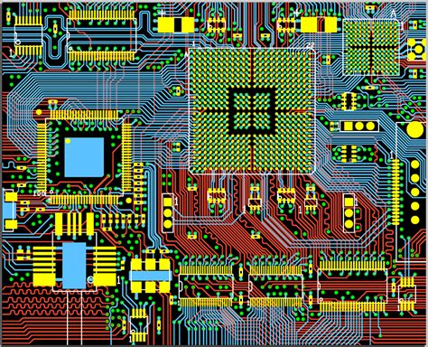
Best Practices for Traces and Routing Techniques
Effective traces and routing techniques are crucial for ensuring the performance and reliability of your printed circuit board (PCB) design. Start by maintaining the shortest possible connections among components to minimize signal loss and potential interference. When selecting trace widths, remember that wider traces can carry more current, but they also take up more space on the board. Utilize the standard trace width calculator based on your circuit requirements to determine appropriate widths for different sections of your design.
Additionally, pay attention to the layer stack-up; using multiple layers can help manage complex routing while reducing electromagnetic interference among traces. Keep sensitive signal lines away from noisy power lines whenever possible; this separation is essential for maintaining signal integrity. Whenever feasible, employ ground planes which provide a low-resistance return path, thereby improving overall circuit performance.
A well-organized routing structure not only enhances performance but also simplifies the manufacturability of your PCB. This is particularly important when considering PCB manufacturing cost; a cleaner design can lead to fewer manufacturing errors, reducing costs associated with rework or scrap materials. When collaborating with PCB manufacturing companies, present clear routing layouts that clearly indicate vital connections.
In conclusion, taking into account these best practices during your PCB design process can significantly influence both functionality and reliability in your final product, making it a critical part of any PCB manufacturing business strategy. For further insights into effective PCB production methods, check out this resource.
Understanding Component Placement for Optimal Performance
Effective component placement is paramount in achieving optimal performance in your PCB design. Start by prioritizing the functionality of the circuit; components that interact frequently should be placed closer together to reduce signal loss and interference. Consider the flow of signals as you position your components; this ensures that traces are kept short and minimizes potential noise issues. A well-placed component layout not only enhances electrical performance but also simplifies the PCB manufacturing process, which is crucial for keeping PCB manufacturing costs manageable.
When evaluating options for PCB manufacturing, it’s wise to consider established PCB manufacturing companies that understand the implications of component placement on both performance and manufacturability. Poorly laid out designs can lead to higher costs during production, affecting the overall PCB manufacturing business model if not carefully managed. You should also think about thermal management; components generating heat should be strategically spaced to allow for effective heat dissipation while maintaining accessibility for assembly and testing.
Incorporating robust design rules during the component layout phase can dramatically impact not only your circuit’s reliability but also its ability to pass testing and quality assurance checks. By understanding these nuances in component placement, you position yourself to create boards that excel in their intended applications while navigating the complexities of production and increasing your competitive edge within the industry.
Strategies for Ensuring Manufacturability and Testing
When it comes to ensuring manufacturability in PCB design, you need to adopt strategies that foster both efficiency and quality throughout the manufacturing process. First and foremost, working closely with PCB manufacturing companies early in the design phase can help you gain insights into potential challenges that may arise during production. By understanding the capabilities and limitations of these companies, you can optimize your layout to align with their processes, which can ultimately lower your PCB manufacturing cost.
In addition, it’s crucial to incorporate testing considerations from day one. Designing with testability in mind not only improves the reliability of your end product but also simplifies the verification process during production. Adding test points and ensuring adequate clearance for probes are effective ways to facilitate this. When you incorporate these elements into your PCB manufacturing business strategy, you enhance the potential for quick identification of faults, minimizing delays that could affect timelines.
Moreover, utilizing software tools that simulate both electrical performance and thermal characteristics can provide invaluable feedback on how components will interact under various conditions. This predictive approach enables you to refine your design before it goes into production, thus reducing errors that could impact manufacturability. Balancing complex designs with practical assembly considerations is key; strive for a layout that accommodates modern manufacturing techniques while also being mindful of future testing procedures. In doing so, you’ll ensure a robust and reliable product ready for market success.
Conclusion: The Future of PCB Design Excellence
As you look towards the future of PCB design, it’s essential to recognize the dynamic landscape shaped by evolving technologies and market needs. The role of PCB manufacturing has become increasingly pivotal in this evolution, influencing both the quality and the cost-effectiveness of designs you create. With an array of PCB manufacturing companies entering the market, competition accelerates innovation and drives down PCB manufacturing costs, enabling you to access advanced materials and processes previously considered beyond reach. To excel in this field, understanding the broader implications of your designs in relation to manufacturing will enhance your ability to create high-performance circuits that are also cost-efficient. Emphasizing both functional reliability and ease of mass production will be crucial in establishing a successful PCB manufacturing business. Ultimately, embracing these principles will not only improve your designs but also strengthen your position in a rapidly advancing technological world, ensuring that your contribution to PCB design excellence fulfills both present demands and future aspirations.
Conclusion: The Future of PCB Design Excellence
As you reflect on the journey toward mastering good PCB design, it’s clear that understanding the pcb manufacturing process plays a vital role in ensuring your layouts are not only effective but also economically viable. Working closely with reputable pcb manufacturing companies can help you grasp the intricacies of production, which can significantly impact the pcb manufacturing cost associated with your projects. This knowledge empowers you to design with manufacturability in mind, thus reducing potential obstacles down the line. By applying best practices discussed throughout this article, you not only enhance your designs but also contribute to a thriving pcb manufacturing business environment where innovation and reliability are paramount. Embrace these guidelines as a roadmap to achieving excellence, ensuring your designs meet the highest standards in performance and manufacturability for future endeavors.

FAQs
Q: What is the importance of PCB manufacturing in electronic design?
A: PCB manufacturing is crucial as it translates your designs into physical products. The quality of your printed circuit boards affects the reliability and performance of the end product.
Q: How can I choose a reliable PCB manufacturing company?
A: When selecting PCB manufacturing companies, consider factors such as their reputation, customer reviews, quality certifications, and the range of services they offer which should align with your specific needs.
Q: What factors influence PCB manufacturing costs?
A: Several elements affect PCB manufacturing cost, including the complexity of your design, the materials used, layer counts, and quantities. More intricate designs typically lead to higher costs due to longer production times and advanced technology requirements.
Q: What is involved in starting a PCB manufacturing business?
A: To start a PCB manufacturing business, you must understand the technical requirements, invest in high-quality machinery, source raw materials effectively, ensure compliance with industry standards, and build a reliable network for sourcing components and distribution.
Q: How can I reduce costs during the PCB design phase?
A: To minimize expenses during PCB design, prioritize efficient layouts by using best practices in routing and component placement. Also consider producing only what you need by understanding your market demands to avoid overspending in PCB manufacturing costs.
For more detailed information about PCB manufacturing, please click here Andwin PCB Manufacturing.