Essential PCB Assembly Drawing Guidelines for Error-Free Manufacturing

Key Takeaways
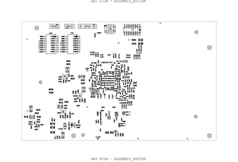
Effective PCB assembly relies on precise documentation, starting with a well-structured assembly drawing. This drawing serves as the blueprint for PCBA manufacturing, ensuring all stakeholders align on component placement, orientation, and critical design specifications. Key elements include clear layer identification, accurate solder mask definitions, and explicit polarity markings for components like diodes or capacitors.
Tip: Always cross-reference the Bill of Materials (BOM) with the assembly drawing to eliminate discrepancies between part numbers and physical placements.
Avoid oversights by double-checking tolerances and dimensional callouts, particularly for high-density layouts. Misaligned pads or unclear fiducial markers can lead to PCBA defects, delaying production. Additionally, adhere to IPC-A-610 or IPC-6012 standards for soldering quality and material compatibility.
Prioritize annotations that specify thermal management zones or ESD-sensitive areas, as these details prevent rework and ensure reliability. Transition smoothly between design and manufacturing phases by integrating feedback loops with your PCB assembly partner. This collaborative approach minimizes errors and streamlines compliance with industry benchmarks.

PCB Assembly Key Components
Understanding the critical elements of PCB assembly is fundamental to achieving reliable PCBA outcomes. The core components include active and passive devices such as integrated circuits (ICs), resistors, capacitors, and connectors, each requiring precise alignment with design specifications. The substrate material (typically FR-4) forms the foundation, while soldermask and silkscreen layers ensure insulation and component labeling accuracy.
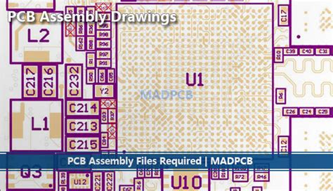
A well-designed PCB assembly drawing must clearly define footprint geometries, polarity markers, and thermal relief patterns to guide manufacturers. For example, Allegro PCB Manufacturing guidelines emphasize the importance of specifying pad sizes and drill hole tolerances to prevent soldering defects. Additionally, surface-mount technology (SMT) and through-hole components demand distinct placement strategies to optimize signal integrity and mechanical stability.
Critical auxiliary elements like test points, fiducial markers, and board edge clearances further enhance manufacturability. By prioritizing these components in PCB assembly documentation, engineers minimize risks of misinterpretation during fabrication, ensuring compliance with IPC-A-610 or J-STD-001 standards. This systematic approach bridges design intent with production reality, laying the groundwork for error-free PCBA workflows.
Avoid PCB Assembly Mistakes
Preventing errors in PCB assembly requires meticulous attention to design specifications and manufacturing workflows. One common pitfall is improper component placement, which can lead to signal interference or mechanical conflicts. To mitigate this, ensure double-checking footprint compatibility between the PCBA design and the bill of materials (BOM). Misaligned solder pads or incorrectly sized apertures, for instance, often result in weak solder joints or tombstoning.
Another critical area is annotation clarity. Ambiguous silkscreen markings or missing polarity indicators increase the risk of assembly errors. Adopt a standardized labeling system, such as IPC-7351 guidelines, to ensure consistency. Below is a table summarizing frequent PCB assembly mistakes and their solutions:
| Error Type | Impact | Prevention Strategy |
|---|---|---|
| Incorrect footprint use | Component misalignment | Verify library models against datasheets |
| Inadequate thermal relief | Poor solder flow | Optimize pad geometry for heat dissipation |
| Missing test points | Limited post-assembly diagnostics | Integrate test points in high-risk areas |
Additionally, thoroughly review design for manufacturability (DFM) checks to identify issues like insufficient clearance between components or non-compliant trace widths. Collaborating with PCBA manufacturers early in the design phase ensures alignment with their capabilities, reducing rework costs. By addressing these factors systematically, engineers can streamline production and minimize defects in PCB assembly workflows.
PCB Design Specs Guide
Effective PCB assembly relies on precise design specifications that align with manufacturing capabilities and industry requirements. At the core of PCBA design, engineers must define critical parameters such as material selection, layer stack-up configurations, and trace width/spacing to ensure signal integrity and mechanical stability. Adherence to standards like IPC-2221 or IPC-7351 is non-negotiable for optimizing solderability and minimizing thermal stress during production.
Key considerations include specifying copper weight for current-carrying capacity, dielectric constants for high-frequency applications, and tolerance thresholds for drill holes and vias. For example, a 0.15mm annular ring ensures reliable plating in dense layouts, while solder mask clearances prevent bridging in fine-pitch components. Designers should also validate thermal management strategies, such as incorporating thermal relief pads or heat sinks, to mitigate overheating risks in PCBA operations.
Transitioning from schematic to physical layout demands rigorous design rule checks (DRC) to flag conflicts like insufficient creepage distances or overlapping pads. Tools like Gerber files and bill of materials (BOM) annotations must align with fabrication guidelines to avoid misinterpretation. By balancing performance requirements with manufacturability, teams achieve a seamless transition from design to PCB assembly, reducing rework and accelerating time-to-market.
Component Placement Strategies
Effective PCB assembly requires strategic component arrangement to balance thermal management, signal integrity, and mechanical stability. Start by grouping components based on functional relationships, such as placing analog and digital circuits in distinct zones to minimize interference. Prioritize PCBA efficiency by positioning high-frequency or heat-generating components (e.g., voltage regulators) away from sensitive devices like sensors, ensuring adequate airflow and thermal relief.
Orientation consistency is critical—align polarized parts (capacitors, diodes) uniformly to reduce placement errors during automated assembly. Maintain minimum clearance between components to prevent solder bridging while avoiding excessive spacing, which complicates trace routing. For surface-mount devices (SMDs), adhere to reflow soldering requirements by aligning pads symmetrically and avoiding shadowing effects.
Incorporate design for manufacturing (DFM) principles by verifying component footprints match datasheet specifications and confirming placement aligns with pick-and-place machine capabilities. Always reference industry-standard guidelines for tolerances and assembly constraints. Finally, validate placements using 3D models to detect mechanical conflicts, such as overlapping connectors or insufficient board-edge clearance, which could delay PCB assembly timelines or increase rework costs.
PCB Annotation Best Practices
Effective annotation is the backbone of clear communication in PCB assembly design, ensuring manufacturers interpret design intent accurately. Start by labeling reference designators (e.g., R1, C2) consistently across silkscreen layers, paired with unambiguous polarity markers for components like diodes or electrolytic capacitors. Critical details such as PCBA orientation indicators, pin-1 identifiers, and thermal management zones must be explicitly marked to prevent placement errors.
Use standardized symbols for ground connections, power rails, and test points to align with industry-standard fabrication practices. Avoid overcrowding annotations by prioritizing essential information—overly dense markings can obscure solder mask layers or complicate automated optical inspection (AOI). For complex assemblies, include assembly notes specifying torque requirements for mechanical parts or special handling instructions for sensitive ICs.
Adopt a hierarchical annotation system: primary labels should dominate silkscreen layers, while secondary details (e.g., firmware version codes) can reside in auxiliary documentation. Always cross-verify annotations against the bill of materials (BOM) to eliminate discrepancies between component values and labeled specifications. By integrating these practices, PCB assembly teams minimize misinterpretation risks, streamline PCBA workflows, and uphold compliance with IPC-7351 or other relevant standards.
PCB Assembly Compliance Standards
Adherence to industry compliance standards is critical for ensuring the reliability and functionality of PCB assembly (PCBA) products. Key regulations, such as IPC-A-610 (Acceptability of Electronic Assemblies) and IPC-J-STD-001 (Requirements for Soldered Electrical Connections), define baseline criteria for solder joint quality, component orientation, and material compatibility. Manufacturers must also align with ISO 9001 for quality management systems and UL certification for safety compliance, particularly in high-risk applications like automotive or medical devices.
To avoid delays or rework, designers should integrate compliance checks early in the PCBA workflow. This includes validating trace spacing against IPC-2221 guidelines, ensuring proper thermal management for components, and specifying RoHS-compliant materials to meet environmental regulations. For instance, a missing halogen-free designation in the assembly drawing could lead to non-compliance with international environmental directives like REACH.
Additionally, clear documentation of tolerance ranges and finish specifications (e.g., ENIG or HASL) in the PCB assembly drawing helps manufacturers avoid misinterpretations. For a deeper dive into design-for-manufacturing (DFM) principles, refer to this comprehensive guide on optimizing layouts for automated assembly. By embedding these standards into the design phase, teams can streamline production while mitigating risks associated with regulatory audits or field failures.
Efficient PCB Assembly Processes
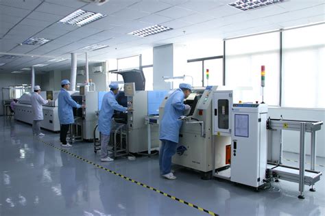
Streamlining PCB assembly workflows requires balancing speed with precision to minimize production delays while maintaining quality. Modern automated pick-and-place systems and reflow soldering technologies form the backbone of PCBA efficiency, enabling rapid component placement with micron-level accuracy. To optimize throughput, manufacturers often implement just-in-time material sourcing paired with digitally validated Bill of Materials (BOM) files, reducing inventory bottlenecks.
Critical process enhancements include:
- Design-for-manufacturing (DFM) checks during pre-production to flag potential assembly conflicts
- Dynamic thermal profiling to ensure consistent solder joint quality across batch runs
- Automated optical inspection (AOI) systems detecting placement errors at 15,000+ components per hour
Lean methodologies like single-piece flow in mixed-product assemblies further reduce turnaround times without compromising PCB assembly standards. For high-density designs, laser-assisted alignment techniques maintain positional tolerances below 50µm, crucial for micro-BGA and QFN packages. By integrating real-time process monitoring with PCBA line analytics, manufacturers achieve defect rates under 50ppm while sustaining 98% equipment utilization rates.
PCB Assembly Testing Protocols
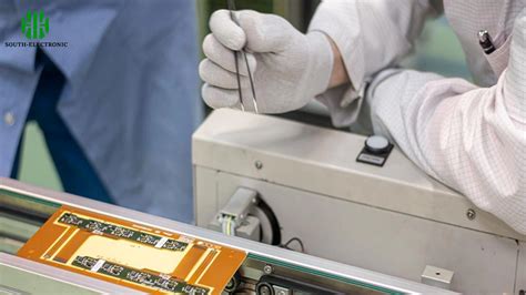
Effective PCB assembly requires rigorous testing protocols to ensure reliability and functionality throughout the production cycle. Critical stages include In-Circuit Testing (ICT) to verify electrical connectivity, Automated Optical Inspection (AOI) for solder joint integrity, and Functional Testing to simulate real-world operating conditions. These protocols validate alignment with assembly drawings and design specifications, identifying discrepancies such as misplaced components or insufficient solder paste application.
For PCBA manufacturers, integrating Design for Testability (DFT) principles during the design phase streamlines fault detection, reducing rework costs. Test coverage should account for IPC-A-610 standards, ensuring compliance with solder quality and component orientation requirements. Additionally, environmental stress testing (e.g., thermal cycling) may be employed to assess durability under extreme conditions.
Clear documentation of test parameters and failure modes in assembly drawings enables traceability and corrective action. Collaboration between design and manufacturing teams ensures testing protocols address both functional performance and manufacturability, minimizing defects in high-volume production. By prioritizing systematic validation, manufacturers mitigate risks while maintaining alignment with industry benchmarks for PCB assembly quality.
Conclusion
Effective PCB assembly relies on meticulous preparation, particularly in creating comprehensive assembly drawings that leave no room for ambiguity. By adhering to industry standards and integrating precise design specifications, manufacturers can mitigate risks of defects and delays. A well-structured PCBA drawing not only clarifies component placement but also ensures alignment between design intent and production execution, reducing costly rework.
Key considerations include validating footprint accuracy, defining solder mask requirements, and specifying critical inspection points. Transitioning from design to manufacturing becomes seamless when annotations explicitly address material compatibility and thermal management constraints. For additional guidance on optimizing assembly documentation, refer to industry-leading practices, which emphasize standardized symbology and layer-specific callouts.
Ultimately, the success of PCB assembly hinges on balancing technical rigor with clarity. Prioritizing collaborative reviews with fabrication partners and leveraging automated verification tools further strengthens process reliability. By treating assembly drawings as dynamic assets—continuously refined through feedback loops—teams can achieve consistent quality across high-volume production runs.
FAQs
What information must a PCB assembly drawing include for manufacturing clarity?
A comprehensive PCB assembly drawing should specify component placements, reference designators, polarity markings, and solder mask requirements. Include critical dimensions, layer stack-up details, and any special instructions for PCBA processes like conformal coating or selective soldering.
How can improper annotations lead to assembly errors?
Ambiguous or missing annotations often cause misaligned components or incorrect orientation. Clear callouts for solder paste layers, fiducial markers, and test points ensure PCB assembly technicians interpret design intent accurately, reducing rework risks.
Why are industry standards like IPC-A-610 crucial in PCBA?
Adherence to IPC-A-610 guarantees acceptable soldering quality and mechanical stability. These standards define acceptance criteria for PCBA outputs, ensuring consistency across batches and minimizing compliance-related delays.
What are common mistakes in component placement strategies?
Overlooking thermal management zones or placing heat-sensitive parts near high-power components often leads to field failures. Always validate clearance rules and assembly tool access during PCB assembly design reviews.
How does testing protocol integration improve PCBA reliability?
Embedding in-circuit test (ICT) or functional test (FCT) requirements in drawings helps manufacturers align inspection processes. This proactive step reduces defect escape rates and ensures PCBA performance matches design specifications.
Streamline Your Next PCB Assembly Project
For tailored PCB assembly solutions that adhere to stringent industry standards, please click here to explore professional services. Ensure seamless translation from design to production with expert PCBA support.


