Expert Double-Sided PCB Manufacturers for Seamless Integration
Key Takeaways
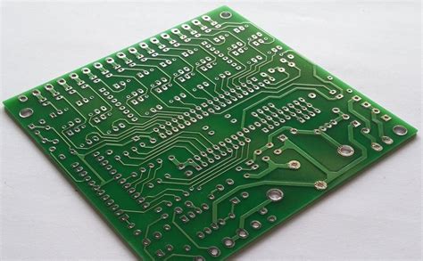
When evaluating PCB manufacturing options, understanding core considerations ensures optimal results for your projects. Double-sided boards offer distinct advantages in circuit density and integration—particularly when working with PCB manufacturing companies that specialize in plated through-hole (PTH) technology. This method enhances electrical connectivity between layers, critical for applications like IoT devices or telecom systems where space constraints demand high-density layouts.
A key factor is PCB manufacturing cost. While dual-layer boards may initially seem pricier than single-sided alternatives, their efficiency in reducing assembly steps often offsets expenses. For example:
| Feature | Single-Sided PCB | Double-Sided PCB |
|---|---|---|
| Layer Complexity | Low | Moderate |
| Component Density | Limited | High |
| Typical Applications | Basic circuits | Advanced systems |
"Choosing a manufacturer with expertise in copper layer optimization ensures reliability without compromising affordability," notes an industry leader in PCB design standards.
To maximize value in your PCB manufacturing business, prioritize partners offering rigorous quality testing and material transparency. This minimizes risks like signal interference or thermal issues. Additionally, consider scalability—reputable providers adapt to evolving needs, whether prototyping or mass production. By balancing technical precision with cost-efficiency, you secure solutions that align with both performance goals and budget constraints.
Dual-Layer PCB Manufacturing Techniques
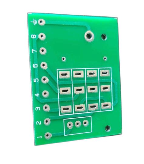
When designing dual-layer PCBs, you need PCB manufacturing techniques that balance precision and scalability. Modern PCB manufacturing companies leverage advanced processes like plated through-holes (PTH) and surface-mount technology (SMT) to create reliable interconnections between copper layers. PTH ensures electrical continuity by metallizing holes drilled through the substrate, while SMT allows compact component placement—critical for minimizing PCB manufacturing cost without sacrificing performance.
To optimize thermal management and signal integrity, manufacturers strategically layer copper traces, often using controlled impedance routing. This approach reduces crosstalk in high-frequency applications, making dual-layer boards ideal for mid-complexity projects. However, managing PCB manufacturing business demands requires balancing material choices—like FR-4 or polyimide substrates—with production volumes. For instance, batch ordering substrates can lower per-unit costs but requires accurate demand forecasting.
Advanced etching techniques, such as laser direct imaging (LDI), further refine trace accuracy, enabling tighter spacing for high-density designs. By collaborating with experienced PCB manufacturing companies, you ensure adherence to industry standards like IPC-A-600, which governs solder mask quality and copper thickness. These techniques not only enhance board reliability but also streamline integration into larger systems—a key consideration for scaling prototypes to mass production.
Cost-Effective Double-Sided PCB Solutions
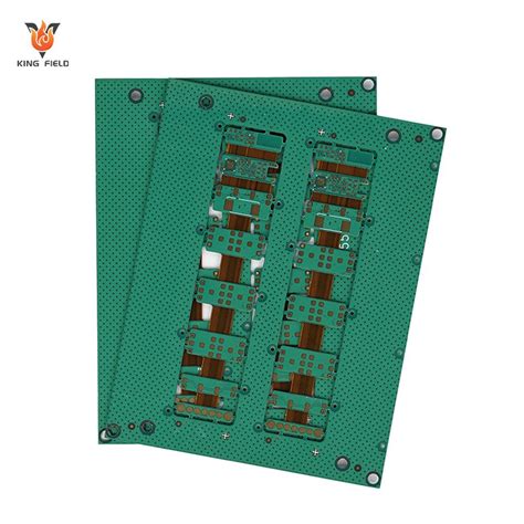
When evaluating PCB manufacturing options for your project, balancing performance and affordability is critical. Double-sided boards inherently reduce PCB manufacturing cost by maximizing circuit density without requiring advanced multilayer processes. Reputable PCB manufacturing companies achieve this through optimized copper layer layouts, minimizing material waste while maintaining signal integrity. By leveraging automated drilling and plating technologies, they ensure precise through-hole connections that eliminate the need for costly manual adjustments.
For businesses managing tight budgets, selecting a PCB manufacturing business with expertise in volume production can further lower per-unit expenses. Advanced panelization techniques allow manufacturers to produce multiple boards simultaneously, reducing overhead. However, cost-effectiveness doesn’t mean compromising quality—top-tier suppliers use rigorous testing protocols to prevent defects that could escalate long-term expenses.
If you’re designing IoT devices or compact consumer electronics, double-sided PCBs offer space-efficient solutions that align with modern miniaturization trends. Partnering with manufacturers that specialize in high-yield fabrication ensures seamless integration of dual-layer designs into your final product. This approach not only streamlines assembly but also accelerates time-to-market—a critical factor in competitive industries where PCB manufacturing efficiency directly impacts profitability.
Plated Through-Hole Technology Explained
Plated through-hole (PTH) technology is a cornerstone of modern PCB manufacturing, enabling reliable electrical connections between dual copper layers. When PCB manufacturing companies drill holes through a board, they electroplate the interior walls with conductive material, creating pathways for signals and power to traverse both sides. This process not only strengthens mechanical stability but also enhances signal integrity in high-frequency applications, a critical factor for industries like telecom and automotive systems.
While PTH increases PCB manufacturing cost due to additional drilling and plating steps, it optimizes space efficiency—a key advantage for compact IoT devices or consumer electronics. Advanced PCB manufacturing business operations leverage automated drilling systems to maintain precision, minimizing errors that could lead to costly rework. However, balancing durability and affordability requires careful material selection, such as choosing epoxy resins that withstand thermal stress during plating.
For projects demanding robust interlayer connectivity, PTH remains unmatched in reliability. By understanding its role in high-density circuit integration, you can better evaluate whether this technology aligns with your design goals and budget constraints.
Space-Efficient PCB Designs for IoT
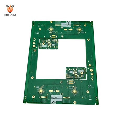
When developing IoT devices, optimizing physical space becomes critical. PCB manufacturing companies leverage dual-layer designs to maximize functionality without expanding the board’s footprint. By strategically routing circuits on both sides of the substrate, high-density layouts reduce the need for additional components, directly lowering PCB manufacturing cost while maintaining performance.
Advanced PCB manufacturing techniques, such as laser-drilled microvias and precision-etched copper layers, enable tighter component placement. This is particularly valuable for IoT applications like wearable sensors or smart home modules, where compactness directly impacts usability. Plated through-holes (PTH) ensure reliable electrical connections between layers, even in ultra-thin boards, supporting seamless integration with wireless communication chips or power management systems.
To balance efficiency and scalability in your PCB manufacturing business, consider material choices like flexible substrates for irregularly shaped devices. Partnering with manufacturers specializing in miniaturized designs ensures compliance with thermal and signal integrity requirements. By prioritizing space-conscious strategies, you can achieve durable, cost-effective solutions tailored for next-generation IoT ecosystems.
High-Density Circuit Board Integration
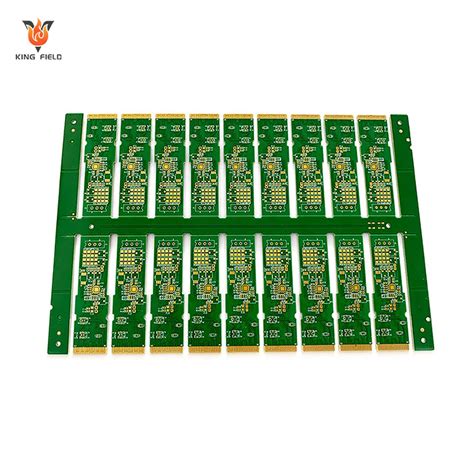
Achieving high-density circuit board integration requires balancing advanced design principles with precision PCB manufacturing processes. By leveraging dual copper layers and plated through-hole (PTH) technology, modern PCB manufacturing companies create boards that maximize component density without compromising reliability. This is critical for applications where space constraints demand compact yet powerful circuitry, such as wearables or industrial automation systems.
When implementing high-density designs, you’ll need to consider how trace width and layer alignment affect signal integrity. Optimizing these parameters ensures minimal crosstalk while maintaining thermal stability—a priority for PCB manufacturing cost efficiency. Advanced techniques like via-in-pad or stacked microvias further enhance routing flexibility, enabling seamless connections between layers even in ultra-thin profiles.
For businesses scaling production, partnering with PCB manufacturing business specialists who understand material selection (e.g., high-Tg substrates) and automated assembly workflows becomes essential. These partnerships not only reduce prototyping risks but also ensure consistent quality across high-volume orders. By prioritizing design-for-manufacturability (DFM) principles, you avoid costly revisions and accelerate time-to-market for densely integrated electronic systems.
Consumer Electronics PCB Applications
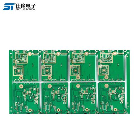
When selecting PCB manufacturing companies for consumer devices, you need solutions that balance performance with compact form factors. Modern smartphones, wearables, and home automation systems rely on dual-layer PCBs to maximize functionality within tight spaces. These boards enable higher circuit density through plated through-hole technology, ensuring reliable connections between layers while maintaining signal integrity in high-frequency applications.
For cost-sensitive projects like smartwatches or IoT sensors, controlling PCB manufacturing cost becomes critical. Reputable manufacturers optimize copper layer layouts to reduce material waste and streamline assembly processes. This efficiency directly impacts your product’s scalability—whether you’re prototyping a fitness tracker or mass-producing wireless earbuds.
The PCB manufacturing business has evolved to address demands for thinner, lighter devices. Advanced etching techniques allow for finer traces, supporting features like touchscreens and biometric sensors. When sourcing boards, prioritize partners with expertise in thermal management and impedance control, as these factors determine long-term reliability in consumer-grade electronics.
By aligning with skilled PCB manufacturing providers, you ensure seamless integration of power management modules, Bluetooth antennas, and microcontrollers—key components driving today’s connected devices. This foundation supports transitions into adjacent sections, such as IoT systems, where space-efficient designs remain equally vital.
Choosing Reliable PCB Manufacturers
When selecting PCB manufacturing companies, you need to assess their technical expertise, quality certifications, and track record in handling projects similar to yours. Look for suppliers with ISO 9001 or IPC-A-600 compliance, as these standards ensure adherence to rigorous production and inspection protocols. A manufacturer’s ability to balance PCB manufacturing cost with performance is critical—request detailed breakdowns of material expenses, labor fees, and testing charges to avoid hidden costs.
Established PCB manufacturing business operations often invest in advanced plating and etching technologies, which directly impact circuit precision and durability. Verify their capacity to scale production without compromising turnaround times, especially for high-volume orders. Prioritize partners offering design-for-manufacturability (DFM) feedback, as this collaboration minimizes errors and optimizes board layouts for space efficiency.
Finally, evaluate their supply chain transparency and customer support responsiveness. Reliable PCB manufacturing providers maintain clear communication channels, from prototyping to bulk delivery, ensuring your IoT or telecom systems integrate seamlessly. By aligning these factors with your project’s technical and budgetary needs, you mitigate risks and secure long-term partnerships for complex electronics development.
Copper Layer Optimization in PCBs
When designing double-sided boards, optimizing copper layers directly impacts performance, durability, and PCB manufacturing cost. Thicker copper traces enhance current-carrying capacity and thermal management, critical for high-power applications like telecom systems. However, excessive copper thickness can complicate etching processes, raising material waste and production time. Reputable PCB manufacturing companies strike a balance by using advanced simulation tools to model current flow and heat distribution, ensuring minimal copper usage without compromising functionality.
Plated through-holes (PTHs) further refine this balance by connecting copper layers on both sides, enabling high-density circuit routing while maintaining structural integrity. By adjusting trace widths and spacing, you reduce signal interference and improve impedance control—key for IoT devices requiring compact, reliable designs.
For cost-sensitive projects, PCB manufacturing businesses often recommend hybrid approaches: pairing standard 1-oz copper for general circuits with localized thickened zones for high-stress areas. This strategy lowers PCB manufacturing expenses while meeting performance benchmarks. Always verify that your supplier employs automated optical inspection (AOI) to detect inconsistencies in copper distribution, preventing latent defects in consumer electronics or industrial equipment.
Conclusion
When selecting PCB manufacturing companies for your projects, understanding the balance between PCB manufacturing cost and quality becomes paramount. By leveraging advanced plated through-hole technology and copper layer optimization, reputable manufacturers ensure your designs achieve seamless integration without compromising performance. Whether you’re developing compact IoT devices or high-density telecom systems, choosing partners with expertise in PCB manufacturing business practices guarantees space-efficient layouts and reliable circuit density.
As you evaluate options, prioritize manufacturers that transparently address PCB manufacturing challenges—from material selection to thermal management—while aligning with your budget constraints. This strategic approach not only streamlines production but also future-proofs your electronics against evolving industry demands. Ultimately, the right partnership transforms complex designs into cost-effective, scalable solutions, solidifying your competitive edge in fast-paced markets.
FAQs
How do double-sided PCBs differ from single-layer designs?
Double-sided PCBs utilize copper layers on both sides, connected through plated through-holes, enabling higher circuit density compared to single-layer boards. This design supports complex applications like IoT devices without increasing physical size.
What factors influence PCB manufacturing cost for dual-layer boards?
Key cost drivers include material quality, board thickness, hole-plating complexity, and surface finish. Partnering with experienced PCB manufacturing companies ensures optimized copper layer usage and reduced waste, balancing performance and affordability.
How do you verify reliability in PCB manufacturing?
Reputable manufacturers implement rigorous testing—such as electrical continuity checks and thermal stress tests—to ensure plated through-holes and solder joints meet industry standards. Always review certifications like ISO 9001 when selecting a PCB manufacturing business.
Can double-sided PCBs be reused for prototype iterations?
Yes, their standardized design allows easy modifications, making them ideal for prototyping. Many PCB manufacturing providers offer rapid turnaround services for iterative testing in consumer electronics or telecom systems.
What industries benefit most from space-efficient PCB designs?
IoT, wearables, and automotive systems prioritize compact layouts. Dual-layer boards with high-density integration minimize footprint while maintaining functionality, a specialty of advanced PCB manufacturing companies.
Ready to Optimize Your Next Project?
For tailored solutions in PCB manufacturing, please click here to connect with experts specializing in cost-effective, high-performance designs.


