Explanation of materials and manufacturing process of FPC soft board
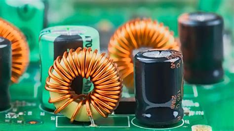
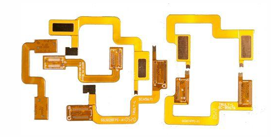
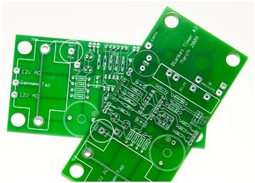
FPC is a flexible circuit board, which belongs to a type of PCB circuit board. FPC soft board is widely used, such as FPCC connector, FPC antenna, wireless charging coil array, etc. So what materials are FPC made of?
1.Raw materials
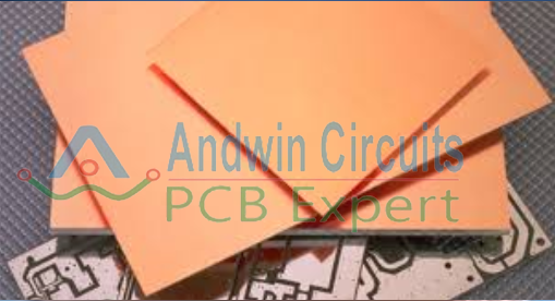
(1) Glue material and non-glue material; the copper on the material is divided into electrolytic copper and rolled copper. The material of non-glue rolled copper is flexible and has better foldability.
(2) Material thickness: PI+copper thickness
2.Covering film
The covering film is composed of PI and glue.
3.Reinforcement
There are generally the following types of reinforcement: PI reinforcement, PET reinforcement, FR4 reinforcement, steel sheet reinforcement, etc. The general reinforcement thickness is PI1/2 1/2, PI11, PI21, PI31 to PI91. The two numbers after PI represent the thickness of PI and the thickness of glue respectively, in Mil. The thickness depends on customer requirements.
4.Pure glue
Pure glue is mainly used for lamination and layering of multilayer boards, and is also used for bonding reinforcement.
5.Screening film
It mainly plays the role of signal shielding, and it must be grounded.
6.3M glue
It is used for bonding reinforcement and fixing FPC.
The process manufacturing process is as follows:
To date, almost all FPC manufacturing processes are processed by subtractive method (etching method). Usually, copper clad board is used as the starting material, and the anti-etching layer is formed by photolithography, and the copper surface of the unwanted part is etched away to form the circuit conductor. Due to problems such as side etching, the etching method has processing limitations for fine circuits.
Then, the sputtering method is used to form a planting layer on the polyimide substrate film, and then the anti-etching layer pattern of the reverse pattern of the circuit is formed on the planting layer by photolithography, which is called the plating resistance layer.
The conductor circuit is formed by electroplating in the blank part. Then remove the anti-etching layer and unnecessary planting layer to form the first layer of circuit. Apply photosensitive polyimide resin on the first layer of circuit, use photolithography to form holes, protective layer or insulating layer for the second layer of circuit, and then sputter to form planting layer on it as the base conductive layer of the second layer of circuit. Repeat the above process to form a multi-layer circuit.
Using this semi-additive method, ultra-fine circuits with a pitch of 5um and a through hole of 10um can be processed. The key to using the semi-additive method to make ultra-fine circuits lies in the performance of the photosensitive polyimide resin used as the insulating layer.
FPC flexible circuit boards have a huge role in the future development. For example, the newly developed bendable screens, mobile phones, computers, automobiles, aviation and other fields are inseparable from flexible circuit boards. What do you think the future development direction of PCB should be?