Explore the impact of several factors on PCB heat dissipation
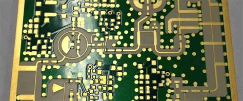
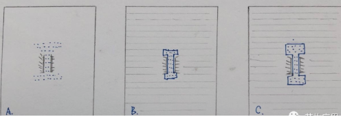
Temperature is one of the key factors that limit device power and performance. Any power chip application engineer must pay attention to the problem of thermal resistance when designing. When θJC is relatively low, the reduction of θJA is particularly important, and the thermal resistance θJA is highly dependent on the design of the PCB. The following takes TSSOP28 as an example and explores the impact of several factors on heat dissipation through several experiments. The figure below A is an ideal board with almost few traces, B is the peripheral traces, relying on the middle heat dissipation pad and upper and lower heat dissipation, and C is to expand the heat dissipation area.
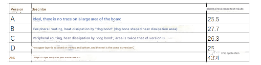
The right side of the table is the thermal resistance test results.
Under the premise of the same vias, 5 boards of the same size are compared, ABCD is a 4-layer board, and the comparison results are shown in the figure above.
Several conclusions can be seen from the results
4-layer boards have a significant heat dissipation effect than 2-layer boards;
Although the dog bond does not help much in heat dissipation in absolute terms, it helps heat dissipation in relative proportion as power consumption increases. It is worth emphasizing that the top layer chip has pins on the left and right that cannot dissipate heat. Try not to run wires in the up and down directions and increase the dog bond area as much as possible.
The solder mask layer on the top and bottom has a heat dissipation effect;
The copper plating area helps heat dissipation;
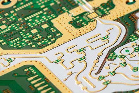
In addition to the above factors, the size, number and through-hole structure of the vias also affect heat dissipation. The figure below shows the effect curve of vias on heat dissipation in 2-layer and 4-layer boards.

As can be seen from the figure, there is a balance point for the number of vias. Too many vias may not improve heat transfer. In addition, this is related to the package size. Take 0.33mm (13mil) vias as an example. The example is as follows
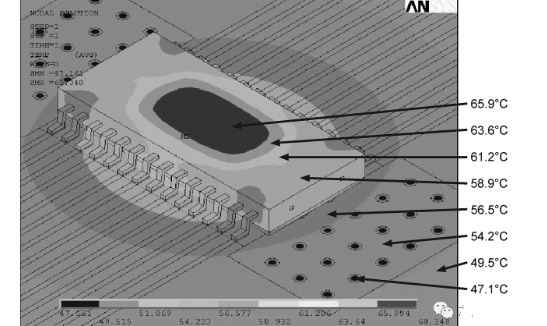
In addition, heat dissipation is conducted from the die to the surrounding area. The following figure is a thermal radiation diagram of a 2-layer board for reference of thermal conductivity design.

The help of schematic design for heat dissipation:
In addition to PCB and heat sink design, we should also pay attention to circuit design. Taking the speaker with battery as an example, the two chips with the highest heat generation are DC-DC boost and power amplifier. In particular, the market demand for power is getting higher and higher, such as the demand for power amplifier output 2X25W (THD+N=1%), which requires a battery boost chip to about 16V.
When the battery voltage is boosted to 16V and the current is continuously increased, the chip efficiency will gradually decrease as the heat rises, and the greater the voltage difference, the lower the efficiency of the boost chip, and the lower the efficiency, the greater the heat generation.
The same principle applies to the power amplifier. The high and low levels of the PWM waveform at the output are PVDD and GND. The higher the PVDD, the lower the efficiency, and the easier it is for the power amplifier to heat up.
Therefore, if the PVDD voltage becomes lower, it can solve the efficiency problem of DCDC and the efficiency problem of the power amplifier, which is a win-win situation with one stone. To achieve this function, you can use the CLASS H function of ACM3108. The principle of this function is as follows:
According to the characteristics of the music signal, ACM3108 provides a control signal to control the FB of the chip, thereby controlling the boost PVDD
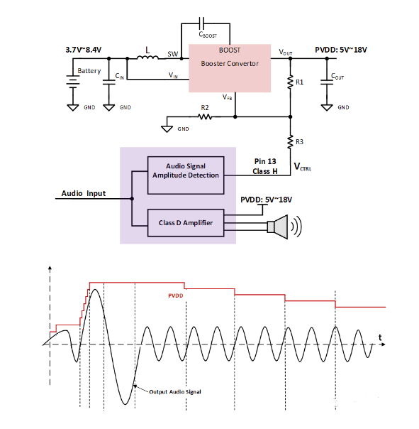
With the change of PVDD, the efficiency of boost and power amplifier are both improved. When playing music, the overall heat generation is greatly reduced, and the playing time is also increased by about 40%.