Exposed Copper on PCBs: Causes, Effects, and Solutions
Introduction
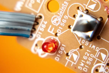
Printed Circuit Boards (PCBs) are the backbone of modern electronics, providing the necessary electrical connections between components. One critical aspect of PCB manufacturing and design is the proper handling of copper traces and pads. However, a common issue that arises is exposed copper, where the copper layer is left unprotected, leading to potential reliability and performance problems.
This article explores the causes, effects, and solutions for exposed copper on PCBs, along with best practices to prevent this issue in PCB fabrication and assembly.
1. What is Exposed Copper on a PCB?
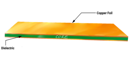
Copper is the primary conductive material used in PCBs, forming traces, pads, and planes that carry electrical signals. To protect copper from oxidation and environmental damage, it is typically covered with a surface finish (e.g., HASL, ENIG, OSP) or a solder mask.
Exposed copper refers to areas where the copper layer is left unprotected due to:
- Improper solder mask application
- Damaged surface finish
- Design or manufacturing defects
If left unaddressed, exposed copper can lead to oxidation, poor solderability, and electrical failures.
2. Causes of Exposed Copper on PCBs
Several factors contribute to exposed copper in PCB manufacturing and assembly:
A. Solder Mask Issues
- Incomplete Coverage: If the solder mask is not properly applied, some copper traces or pads may remain exposed.
- Misalignment: Incorrect solder mask alignment during the manufacturing process can leave copper areas unprotected.
- Cracking or Peeling: Mechanical stress or poor adhesion can cause the solder mask to crack or peel, exposing underlying copper.
B. Surface Finish Defects
- Insufficient Plating: If the surface finish (e.g., ENIG, HASL) is not uniformly applied, some copper areas may remain bare.
- Scratches or Abrasions: Handling damage during PCB fabrication or assembly can scrape off the protective finish.
C. PCB Design Errors
- Insufficient Solder Mask Expansion: If the solder mask clearance is too tight, it may not fully cover copper pads or traces.
- Missing Solder Mask on Non-Solderable Areas: Some designers forget to apply solder mask on non-critical copper pours, leaving them exposed.
D. Environmental and Handling Factors
- Oxidation Over Time: If a PCB is stored improperly, moisture and oxygen can degrade the surface finish, exposing copper.
- Chemical Exposure: Harsh cleaning agents or flux residues can corrode the protective layers.
3. Effects of Exposed Copper on PCBs
Exposed copper can lead to multiple reliability and performance issues:
A. Oxidation and Corrosion
Copper readily reacts with oxygen and moisture, forming copper oxide (CuO/Cu₂O), which is non-conductive. This can result in:
- Increased resistance in traces
- Poor solderability
- Intermittent connections or open circuits
B. Solderability Problems
Exposed copper surfaces may oxidize before assembly, leading to:
- Poor wetting during soldering
- Weak solder joints
- Tombstoning or voiding in reflow processes
C. Electrical Shorts and Leakage
If exposed copper is near other conductive elements, it can cause:
- Dendritic growth (electrochemical migration)
- Current leakage
- Short circuits due to solder bridging
D. Reduced PCB Lifespan
Corroded copper traces weaken over time, leading to:
- Cracked traces under thermal cycling
- Premature PCB failure
4. Solutions to Prevent and Fix Exposed Copper
To mitigate exposed copper issues, PCB manufacturers and designers must follow best practices:
A. Proper Solder Mask Application
- Ensure adequate solder mask expansion (typically 0.05mm–0.1mm beyond pads).
- Use LPI (Liquid Photoimageable) solder mask for better coverage.
- Perform AOI (Automated Optical Inspection) to detect mask defects.
B. Choosing the Right Surface Finish
- ENIG (Electroless Nickel Immersion Gold): Provides excellent oxidation resistance.
- OSP (Organic Solderability Preservative): A cost-effective option for short-term protection.
- Immersion Silver/Tin: Good for high-frequency applications but requires careful handling.
C. PCB Design Best Practices
- Define solder mask dams between fine-pitch components.
- Avoid large exposed copper areas unless necessary (e.g., for heat dissipation).
- Use teardrops at trace-to-pad junctions to prevent mask peeling.
D. Handling and Storage
- Store PCBs in moisture-barrier bags with desiccants.
- Avoid touching copper surfaces with bare hands to prevent oxidation.
- Use conformal coating for added protection in harsh environments.
E. Repairing Exposed Copper
If exposed copper is detected, possible fixes include:
- Localized solder mask touch-up with UV-curable epoxy.
- Reapplying surface finish (e.g., immersion gold or silver).
- Cleaning and tarnishing removal with mild acid solutions (e.g., vinegar or specialized PCB cleaners).
5. Case Study: Exposed Copper in High-Humidity Environments
A consumer electronics manufacturer faced repeated failures in a humid climate. Analysis revealed that exposed copper traces on the PCB were corroding due to moisture ingress. The solution involved:
- Switching from HASL to ENIG for better corrosion resistance.
- Adding conformal coating on assembled boards.
- Improving storage conditions with nitrogen-packed sealing.
Result: Field failure rates dropped by 70% after implementation.
6. Conclusion
Exposed copper on PCBs is a preventable yet critical issue that can lead to oxidation, poor solderability, and electrical failures. By following proper design rules, selecting appropriate surface finishes, and ensuring careful handling, manufacturers can significantly reduce the risk of exposed copper.
For high-reliability applications, additional protective measures such as conformal coating or enhanced solder mask techniques should be considered. By addressing exposed copper proactively, PCB reliability and longevity can be greatly improved.