Exposed Copper PCB: Design, Benefits, and Applications
Introduction to Exposed Copper PCBs
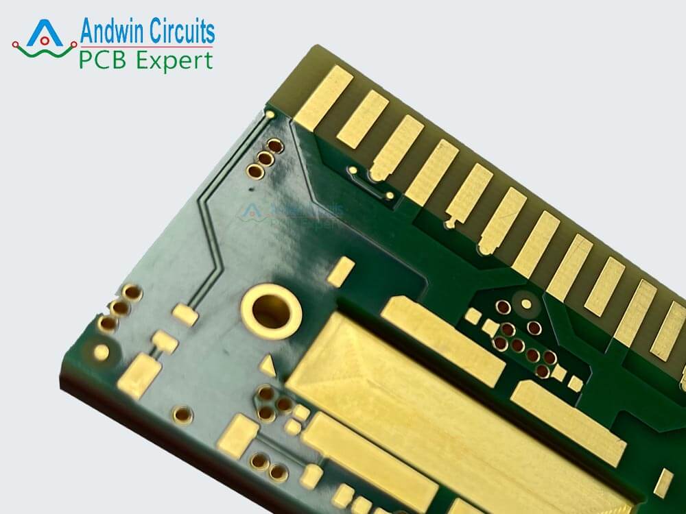
Exposed copper printed circuit boards (PCBs) represent a specialized type of circuit board where portions of the copper layer remain uncovered by solder mask or other protective coatings. This intentional exposure of copper traces and pads serves various functional and aesthetic purposes in modern electronics. Unlike traditional PCBs where all copper surfaces are protected, exposed copper designs leave selected areas bare, creating unique opportunities and challenges for designers and manufacturers.
The concept of exposed copper PCBs has gained significant traction in recent years as electronic devices become more sophisticated and demand higher performance. This technology bridges the gap between standard PCB manufacturing and specialized requirements for thermal management, high-current applications, and distinctive visual appearances. The exposed copper areas can be treated with different surface finishes or left in their natural state, depending on the intended application.
Design Considerations for Exposed Copper PCBs
Layout and Trace Configuration
Designing exposed copper PCBs requires careful planning to balance electrical performance with manufacturability. Engineers must consider:
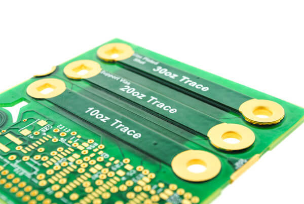
- Trace width calculations: Exposed copper traces often carry higher currents, requiring proper sizing to prevent overheating
- Spacing requirements: Increased clearance between exposed copper features prevents unintended bridging during soldering
- Thermal relief patterns: Critical for components that may need rework or replacement
- Copper balancing: Essential to prevent warping during manufacturing processes
Solder Mask Definition
The solder mask application becomes particularly crucial in exposed copper designs:
- Precision alignment: Required to ensure clean transitions between covered and exposed areas
- Solder mask dams: Narrow strips that prevent solder migration between pads
- Edge clearance: Adequate spacing between copper features and board edges
- Aperture design: Shapes and sizes of openings in the solder mask layer
Surface Finish Selection
Choosing the right surface finish affects both performance and longevity:
- HASL (Hot Air Solder Leveling): Traditional finish, cost-effective but with thickness variations
- ENIG (Electroless Nickel Immersion Gold): Flat surface ideal for fine-pitch components
- OSP (Organic Solderability Preservative): Thin, economical coating for temporary protection
- Immersion Silver: Good conductivity with moderate durability
- Bare copper: Maximum conductivity but requires careful handling to prevent oxidation
Manufacturing Process for Exposed Copper PCBs
Base Material Preparation
The manufacturing process begins with selecting appropriate substrate materials:
- FR-4: Standard epoxy laminate for most applications
- High-Tg materials: For improved thermal performance
- Metal core substrates: When exceptional heat dissipation is required
- Flexible materials: For dynamic or space-constrained applications
Copper Cladding and Patterning
The copper exposure process involves several precise steps:
- Laminate cleaning: Ensures proper adhesion of photoresist
- Photoresist application: Uniform coating for pattern transfer
- Exposure and development: Creates the protective pattern for etching
- Etching process: Removes unwanted copper while protecting desired traces
- Resist stripping: Cleans the board for subsequent processes
Solder Mask Application
Specialized techniques create precise exposed areas:
- Liquid photoimageable solder mask (LPSM): Most common method for high precision
- Dry film solder mask: Alternative for certain applications
- Screen printing: For less complex designs
- Curtain coating: Efficient for high-volume production
Surface Finish Application
Final protective treatments are applied to exposed copper:
- Selective application: Only on designated exposed areas
- Plating thickness control: Critical for consistent performance
- Quality inspection: Verifies complete coverage and uniformity
Benefits of Exposed Copper PCBs
Enhanced Thermal Performance
Exposed copper significantly improves heat dissipation:
- Direct heat path: Eliminates insulating solder mask barrier
- Increased thermal mass: Copper acts as heat sink
- Improved convection: Bare copper enhances airflow cooling
- Efficient heat spreading: Reduces localized hot spots
Superior Electrical Characteristics
Bare copper offers electrical advantages:
- Lower impedance: Absence of solder mask reduces dielectric effects
- Higher current capacity: Increased conductor cross-section
- Reduced skin effect: Especially beneficial for high-frequency applications
- Improved grounding: Better contact with shielding elements
Mechanical and Reliability Advantages
Exposed copper enhances structural integrity:
- Stronger solder joints: Direct copper-to-component connections
- Improved durability: Resists mechanical stress better than coated traces
- Better wire bonding: Essential for certain packaging technologies
- Enhanced repairability: Easier rework and modification
Aesthetic and Functional Design Flexibility
Exposed copper enables unique design possibilities:
- Distinctive appearance: Metallic accents for visual appeal
- Custom branding opportunities: Exposed copper logos or markings
- Tactile features: Different surface textures for user interfaces
- Functional contacts: For switches or test points
Applications of Exposed Copper PCBs
Power Electronics
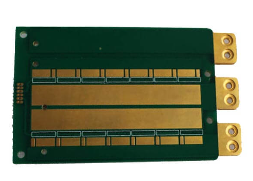
Exposed copper excels in high-power applications:
- Power supplies: Improved current handling and heat dissipation
- Motor controllers: Enhanced thermal management
- Inverters/converters: Better efficiency in energy conversion
- Battery management systems: Robust power distribution
LED Lighting Systems
Thermal management is critical for LED performance:
- High-power LED arrays: Prevents lumen depreciation
- Automotive lighting: Withstands harsh environments
- Architectural lighting: Combines function with aesthetics
- Street lighting: Long-term reliability in outdoor conditions
Automotive Electronics
Exposed copper meets demanding automotive requirements:
- Engine control units: Handles under-hood temperatures
- Power distribution modules: Manages high currents reliably
- Sensor interfaces: Stable signal integrity
- Infotainment systems: Combination of performance and design
Industrial Equipment
Robust performance for industrial environments:
- Motor drives: Sustained high-current operation
- Power converters: Efficient energy transformation
- Control systems: Reliable operation in harsh conditions
- Test equipment: Durable measurement interfaces
Consumer Electronics
Blending performance with aesthetics:
- Audio equipment: Improved signal integrity
- Gaming hardware: Thermal management for high-performance chips
- Wearable devices: Space-efficient thermal solutions
- Smart home devices: Reliable power distribution
Challenges and Solutions in Exposed Copper PCB Implementation
Oxidation Prevention
Bare copper is prone to oxidation, requiring specific strategies:
- Protective coatings: Thin organic preservatives
- Plating options: Selective gold or silver plating
- Storage conditions: Controlled humidity environments
- Assembly timing: Rapid turnaround after fabrication
Solderability Concerns
Maintaining reliable solder connections:
- Surface preparation: Proper cleaning before assembly
- Flux selection: Appropriate for exposed copper
- Reflow profiles: Optimized for bare copper surfaces
- Inspection criteria: Adjusted for exposed copper features
Manufacturing Tolerances
Precision requirements for exposed copper designs:
- Registration accuracy: Critical for solder mask openings
- Etch compensation: Accounting for sidewall etching
- Copper thickness control: Consistent electrical performance
- Quality verification: Specialized inspection techniques
Cost Considerations
Balancing performance with economics:
- Material selection: Premium substrates vs. standard FR-4
- Process complexity: Additional manufacturing steps
- Yield impacts: Potential for increased scrap rates
- Volume effects: Economies of scale in production
Future Trends in Exposed Copper PCB Technology
Advanced Materials Development
Emerging materials will enhance exposed copper performance:
- Nanocomposite coatings: For oxidation protection
- Graphene-enhanced copper: Improved conductivity
- High-thermal-conductivity substrates: Better heat spreading
- Self-healing coatings: For long-term reliability
Manufacturing Innovations
New production techniques will emerge:
- Additive processes: For precise copper deposition
- Laser direct imaging: Improved solder mask accuracy
- Automated optical inspection: Enhanced quality control
- Environmentally friendly processes: Reduced chemical usage
Design Integration
Exposed copper in broader system contexts:
- Embedded components: Within exposed copper structures
- 3D packaging: Integration with exposed thermal paths
- Hybrid circuits: Combining different technologies
- Multi-functional surfaces: Electrical, thermal, and mechanical roles
Sustainability Focus
Environmental considerations will shape development:
- Recycling processes: For copper recovery
- Lead-free alternatives: In surface finishes
- Energy-efficient manufacturing: Reduced carbon footprint
- Longer product lifetimes: Through improved reliability
Conclusion
Exposed copper PCBs represent a significant advancement in printed circuit board technology, offering unique benefits that address the growing demands of modern electronics. From enhanced thermal management to improved electrical performance and distinctive aesthetic possibilities, these specialized PCBs continue to find new applications across diverse industries. While implementation challenges exist, ongoing advancements in materials, manufacturing processes, and design methodologies are steadily overcoming these limitations.
As electronic devices push the boundaries of power density, miniaturization, and functionality, exposed copper PCB technology will play an increasingly vital role. Designers and engineers who master the intricacies of exposed copper implementation will gain access to powerful tools for creating innovative, high-performance electronic products. The future of exposed copper PCBs appears bright, with continued evolution promising even greater capabilities and broader applications in the electronics landscape.


