Failure Analysis of PCB/PCBA Products: Causes, Detection, and Prevention
Abstract
Printed Circuit Boards (PCBs) and Printed Circuit Board Assemblies (PCBAs) are critical components in modern electronic devices. However, failures in these components can lead to significant performance issues, financial losses, and safety hazards. This paper explores common failure modes in PCB/PCBA products, their root causes, detection methods, and preventive measures. By understanding these factors, manufacturers can improve product reliability and reduce failure rates.
1. Introduction
PCBs and PCBAs serve as the backbone of electronic systems, providing mechanical support and electrical connectivity. Despite advancements in manufacturing technologies, failures still occur due to design flaws, material defects, manufacturing errors, and environmental stressors. A systematic approach to failure analysis helps identify root causes and implement corrective actions.
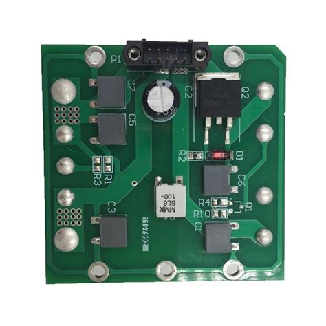
2. Common Failure Modes in PCB/PCBA
2.1. Electrical Failures
- Open Circuits: Broken traces due to mechanical stress, poor soldering, or corrosion.
- Short Circuits: Unintended connections caused by solder bridging, conductive debris, or design errors.
- Intermittent Connections: Loose components or cracked solder joints leading to sporadic functionality.
2.2. Mechanical Failures
- Delamination: Separation of PCB layers due to moisture absorption or thermal stress.
- Cracks in Traces or Substrate: Mechanical bending, shock, or vibration-induced fractures.
- Component Breakage: Physical damage to resistors, capacitors, or ICs during handling or operation.
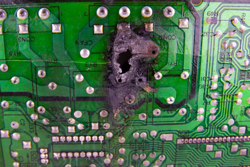
2.3. Thermal Failures
- Solder Joint Fatigue: Repeated thermal cycling weakens solder connections, leading to cracks.
- Overheating: Excessive current or poor heat dissipation causing component degradation.
2.4. Environmental Failures
- Corrosion: Exposure to humidity, chemicals, or contaminants leading to conductive paths or open circuits.
- Electrochemical Migration: Dendritic growth between conductors due to ionic contamination.
2.5. Manufacturing Defects
- Poor Soldering: Cold solder joints, voids, or insufficient wetting.
- Misaligned Components: Incorrect placement leading to poor electrical contact.
- Contamination: Flux residues or foreign materials causing leakage currents or corrosion.
3. Root Causes of PCB/PCBA Failures
3.1. Design-Related Causes
- Insufficient Trace Width: Overheating due to high current density.
- Poor Thermal Management: Lack of heat sinks or improper via design.
- Inadequate Spacing: Risk of short circuits or arcing.
3.2. Material-Related Causes
- Low-Quality Substrates: Poor FR4 material leading to delamination or warping.
- Incompatible Materials: CTE (Coefficient of Thermal Expansion) mismatch causing stress fractures.
3.3. Process-Related Causes
- Improper Reflow Profile: Solder defects due to incorrect temperature settings.
- Insufficient Cleaning: Residual flux causing corrosion or electrochemical migration.
3.4. Operational and Environmental Causes
- Excessive Vibration or Shock: Mechanical stress leading to cracked components.
- Humidity and Contaminants: Accelerated corrosion and leakage currents.
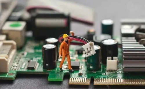
4. Failure Detection and Analysis Techniques
4.1. Visual Inspection
- Microscopy: Identifying cracks, solder defects, or contamination.
- X-Ray Inspection: Detecting hidden solder voids or internal layer defects.
4.2. Electrical Testing
- Continuity Testing: Checking for open or short circuits.
- In-Circuit Testing (ICT): Validating component functionality.
4.3. Thermal Analysis
- Infrared Thermography: Detecting hotspots indicating poor thermal management.
4.4. Advanced Analytical Techniques
- Scanning Electron Microscopy (SEM): Examining microstructure of failed solder joints.
- Energy-Dispersive X-ray Spectroscopy (EDS): Identifying contaminants or corrosion products.
5. Preventive Measures and Best Practices
5.1. Design Improvements
- Optimized Trace Layout: Ensuring proper current-carrying capacity.
- Thermal Relief Pads: Reducing thermal stress on solder joints.
5.2. Material Selection
- High-Tg (Glass Transition Temperature) Substrates: Enhancing thermal stability.
- Conformal Coatings: Protecting against moisture and contaminants.
5.3. Process Optimization
- Controlled Reflow Soldering: Preventing tombstoning or cold solder joints.
- Automated Optical Inspection (AOI): Early defect detection.
5.4. Environmental Protection
- Hermetic Sealing: For high-humidity applications.
- Proper Storage Conditions: Preventing moisture absorption before assembly.
6. Conclusion
PCB/PCBA failures can arise from multiple factors, including design flaws, material defects, manufacturing errors, and operational stresses. A comprehensive failure analysis approach involving visual, electrical, and advanced analytical techniques helps identify root causes. Implementing preventive measures such as improved design practices, material selection, and process controls can significantly enhance reliability. Continuous monitoring and testing are essential to minimize failure risks in critical electronic applications.