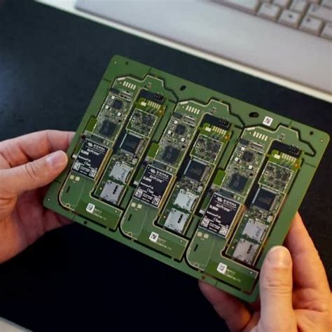
Files needed for pcb assembly
Bill Of Materials (BOM)
Files needed for pcb assembly,such as the Bill of Materials (BOM) is a critical document in the process of Printed Circuit Board (PCB) assembly, serving as a comprehensive list of all the components required to build the PCB.
This document is indispensable for ensuring that the assembly process proceeds smoothly and efficiently. It provides detailed information about each component, including part numbers, descriptions, quantities, and specifications. The BOM acts as a blueprint for the procurement and assembly teams, guiding them through the intricate process of sourcing and placing components on the PCB.
To begin with, the BOM must include the part number for each component.
This unique identifier is essential for distinguishing between different components, especially when they have similar names or functions. The part number allows for precise identification and helps avoid any confusion during the procurement process. Additionally, it facilitates communication between the design team and suppliers, ensuring that the correct components are ordered and delivered.
Moreover, the BOM should provide a detailed description of each component.
This description typically includes the component’s type, value, tolerance, and any other relevant specifications. For instance, a resistor’s description might include its resistance value, tolerance, and power rating. This information is crucial for the assembly team, as it ensures that each component is correctly identified and placed on the PCB according to the design specifications.
In addition to part numbers and descriptions, the BOM must specify the quantity of each component required for the assembly.
This information is vital for inventory management, as it helps the procurement team order the correct number of components. It also aids in cost estimation, allowing the project manager to budget accurately for the assembly process. Furthermore, specifying quantities helps prevent shortages or excesses, both of which can lead to delays and increased costs.
Another important aspect of the BOM is the inclusion of supplier information.
This section lists the preferred suppliers for each component, along with their contact details and part numbers. By providing this information, the BOM streamlines the procurement process, enabling the procurement team to quickly and efficiently source the necessary components. It also helps maintain consistency in component quality, as the same suppliers are used for each production run.
Additionally, the BOM should include reference designators for each component.
These designators correspond to the labels used in the PCB layout, such as R1 for a resistor or C1 for a capacitor. Reference designators are crucial for the assembly team, as they provide a clear and unambiguous way to identify where each component should be placed on the PCB. This ensures that the assembly process is accurate and that the final product functions as intended.
Furthermore, the BOM may include additional notes or comments that provide further guidance for the assembly team.
These notes might include special instructions for handling certain components, such as those that are sensitive to static electricity or require specific orientation. By including these notes, the BOM helps prevent assembly errors and ensures that the final product meets the required quality standards.
In conclusion, the Bill of Materials (BOM) is an essential document for PCB assembly, providing detailed information about each component required for the process. By including part numbers, descriptions, quantities, supplier information, reference designators, and additional notes, the BOM ensures that the assembly process is efficient, accurate, and cost-effective. This comprehensive document serves as a vital link between the design, procurement, and assembly teams, facilitating smooth communication and coordination throughout the PCB assembly process.
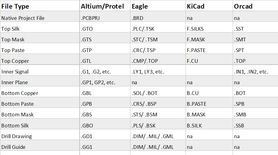
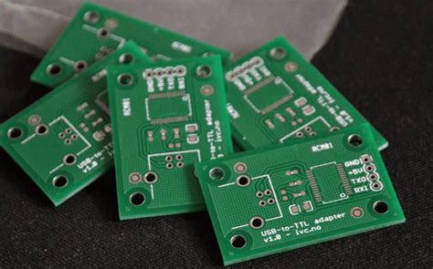
Gerber Files
Gerber files are an essential component in the process of printed circuit board (PCB) assembly, serving as the blueprint for the manufacturing and assembly of the PCB. These files contain all the necessary information required to produce the physical board, including the layout of the copper layers, solder mask, silkscreen, and other critical elements. Understanding the importance and content of Gerber files is crucial for anyone involved in PCB design and manufacturing.
To begin with, Gerber files are a standard format used in the electronics industry to describe the various layers of a PCB.
Each layer of the PCB is represented by a separate Gerber file, and these files collectively provide a comprehensive view of the board’s design. The copper layers, which form the electrical connections on the PCB, are among the most critical files. These layers include the top and bottom copper layers, as well as any internal layers in multi-layer boards. The Gerber files for these layers detail the precise placement and routing of the copper traces, pads, and vias, ensuring that the electrical connections are accurately reproduced during manufacturing.
In addition to the copper layers, Gerber files also include information about the solder mask and silkscreen layers.
The solder mask is a protective layer that covers the copper traces, preventing solder bridges and short circuits during the assembly process. The Gerber file for the solder mask defines the areas where the mask should be applied and where it should be left open to expose the copper pads for soldering. The silkscreen layer, on the other hand, contains text and symbols that provide important information about the components and their placement on the PCB. This layer is typically used to print reference designators, component outlines, and other markings that aid in the assembly and troubleshooting of the board.
Furthermore, Gerber files also include information about the board outline and any mechanical features, such as cutouts, slots, and mounting holes.
The board outline file defines the shape and size of the PCB, ensuring that it fits correctly within the intended enclosure or system. Mechanical features are critical for the proper assembly and functionality of the PCB, and their accurate representation in the Gerber files is essential for the manufacturing process.
It is also important to note that Gerber files are typically accompanied by a drill file, which provides information about the locations and sizes of the holes to be drilled in the PCB. These holes are used for mounting components, creating vias, and attaching connectors. The drill file ensures that the holes are accurately placed and drilled to the correct specifications, which is vital for the proper assembly and functionality of the PCB.
In conclusion, Gerber files are a fundamental part of the PCB assembly process, providing detailed information about the various layers and features of the board. They ensure that the PCB is manufactured and assembled accurately, meeting the design specifications and functional requirements. By understanding the content and importance of Gerber files, designers and manufacturers can work together more effectively to produce high-quality PCBs that meet the needs of their applications.
Pick And Place File
In the realm of printed circuit board (PCB) assembly, the pick and place file is an indispensable component that ensures the accurate placement of electronic components onto the board. This file, often referred to as the centroid file or XY data file, contains critical information that guides automated machinery in the precise positioning of each component. Understanding the structure and significance of the pick and place file is essential for anyone involved in PCB design and manufacturing.
The pick and place file is typically generated during the PCB design process using electronic design automation (EDA) software.
This file includes a detailed list of all the components to be placed on the PCB, along with their exact coordinates, rotation angles, and reference designators. The coordinates are usually specified in either millimeters or inches, depending on the design specifications. These coordinates correspond to the center of each component, hence the term “centroid file.”
One of the primary functions of the pick and place file is to facilitate the automation of the assembly process.
Automated pick and place machines rely on this file to accurately position components on the PCB. The file ensures that each component is placed in the correct location and orientation, which is crucial for the functionality of the final product. Without this file, the assembly process would be prone to errors, leading to potential malfunctions and increased production costs.
Moreover, the pick and place file plays a vital role in quality control.
By providing a precise map of component placements, it allows for thorough inspection and verification of the assembled PCB. This verification process can be automated as well, using optical inspection systems that compare the actual placements with the data in the pick and place file. Any discrepancies can be quickly identified and corrected, ensuring that the final product meets the required standards.
In addition to its role in automation and quality control, the pick and place file is also essential for communication between different stakeholders in the PCB assembly process.
Designers, manufacturers, and assemblers all rely on this file to ensure that they are working with accurate and consistent information. This shared understanding helps to streamline the assembly process, reducing the likelihood of errors and misunderstandings.
Furthermore, the pick and place file can be used to optimize the assembly process. By analyzing the data in the file, manufacturers can identify opportunities to improve efficiency and reduce production time. For example, they can adjust the sequence in which components are placed to minimize the movement of the pick and place machine, thereby speeding up the assembly process. This optimization can lead to significant cost savings, particularly in high-volume production runs.
It is also worth noting that the pick and place file must be kept up to date throughout the design and manufacturing process.
Any changes to the PCB design, such as modifications to component placements or rotations, must be reflected in the file. Failure to update the file can result in incorrect placements and potential defects in the final product. Therefore, maintaining an accurate and current pick and place file is a critical aspect of PCB assembly.
In conclusion, the pick and place file is a fundamental element of PCB assembly, serving multiple functions that are crucial for the successful production of electronic devices. It ensures accurate component placement, facilitates quality control, enhances communication among stakeholders, and enables process optimization. By understanding and effectively utilizing this file, manufacturers can achieve higher efficiency, lower costs, and improved product quality.
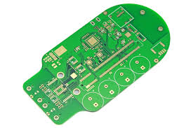
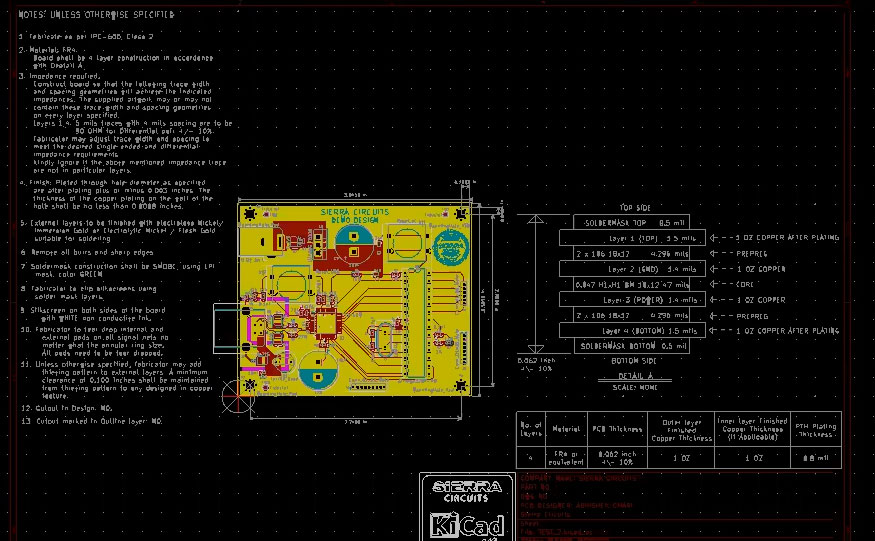
Assembly Drawing
In the realm of printed circuit board (PCB) assembly, the assembly drawing is a critical document that serves as a comprehensive guide for the manufacturing process. This drawing provides detailed instructions and visual representations necessary for the accurate placement and soldering of components onto the PCB. To ensure a seamless transition from design to production, it is essential to understand the various elements that constitute an effective assembly drawing.
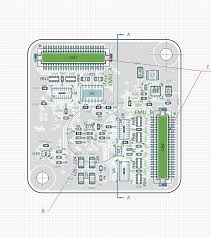
Firstly, the assembly drawing must include a clear and precise depiction of the PCB layout.
This visual representation should highlight the exact locations of all components, including resistors, capacitors, integrated circuits, and connectors. By providing a top-down view of the board, the drawing allows assembly technicians to identify where each component should be placed. Additionally, it is beneficial to include a bottom view if the PCB has components on both sides. This dual perspective ensures that no component placement is overlooked during the assembly process.
Moreover, the assembly drawing should incorporate a bill of materials (BOM) that lists all the components required for the PCB.
The BOM should be detailed, specifying part numbers, descriptions, quantities, and reference designators. This information is crucial for inventory management and ensures that the correct components are used during assembly. Furthermore, the BOM should be cross-referenced with the PCB layout to facilitate easy identification and placement of components.
In addition to the layout and BOM, the assembly drawing must provide detailed assembly notes.
These notes offer specific instructions and guidelines that are not immediately apparent from the visual representation alone. For instance, they may include information on component orientation, soldering techniques, and any special handling requirements for sensitive components. By including these notes, the assembly drawing helps to mitigate potential errors and ensures that the assembly process adheres to the design specifications.
Another important aspect of the assembly drawing is the inclusion of a legend or key.
This legend should explain the various symbols and notations used in the drawing, such as polarity indicators, test points, and reference designators. By providing a clear explanation of these symbols, the legend ensures that assembly technicians can accurately interpret the drawing and execute the assembly process correctly.
Furthermore, the assembly drawing should highlight any critical areas of the PCB that require special attention.
For example, it may indicate regions that are sensitive to electrostatic discharge (ESD) or areas that require precise soldering techniques. By emphasizing these critical areas, the drawing helps to prevent damage to the PCB and ensures that the final product meets the required quality standards.
To facilitate communication and collaboration between the design and assembly teams, the assembly drawing should also include revision history.
This history documents any changes or updates made to the drawing, ensuring that all stakeholders are aware of the latest design modifications. By maintaining an accurate revision history, the assembly drawing helps to prevent discrepancies and ensures that the assembly process is based on the most current design information.
In conclusion, the assembly drawing is an indispensable document in the PCB assembly process. By providing a detailed layout, comprehensive BOM, clear assembly notes, explanatory legend, and highlighting critical areas, the drawing serves as a vital guide for assembly technicians. Moreover, by including revision history, it ensures effective communication and collaboration between design and assembly teams. Ultimately, a well-prepared assembly drawing is essential for achieving a high-quality, reliable PCB that meets the intended design specifications.