Five steps to copy PCB
PCB copy means to reverse analyze the circuit board by reverse technical means on the premise that there are electronic products and circuit boards, and restore the original product’s PCB files, bill of materials, schematics and other technical files 1:1, and then use these technical files and production files to make PCB boards, solder components, debug circuit boards, and complete the entire copy of the original circuit sample.
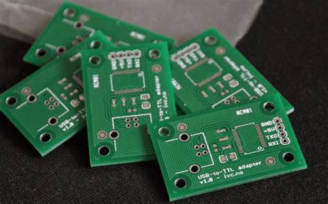
First, take a PCB board.
First, you need to record the model, parameters and position of all components on paper, especially the direction of diodes and triodes, and the direction of IC gaps. It is best to take two photos of the position of components with a digital camera.
Second, remove all components and remove the tin in the PAD hole.
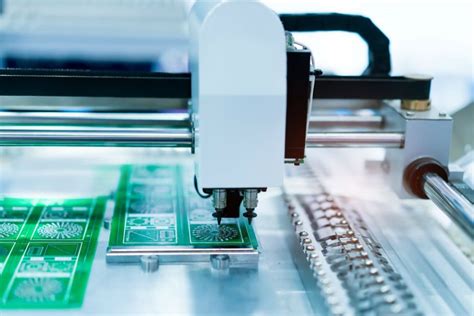
Clean the board with alcohol, and then put it into the scanner. When scanning, slightly increase the scanning pixel to get a clearer board image. Then use water gauze paper to lightly polish the top and bottom layers until the copper film is shiny, put it into the scanner, start PHOTOSHOP, and scan the two layers in color. Note that the PCB must be placed horizontally and vertically in the scanner, otherwise the scanned image cannot be used.
- Adjust the contrast and brightness of the canvas to make a strong contrast between the part with copper film and the part without copper film, then convert the image to black and white, check whether the lines are clear, if not, continue to adjust. If it is clear, save the image as two black and white BMP format files. If there is a problem with the graphics, you need to use PHOTOSHOP to correct it.
- Convert the two BMP format files to PROTEL format files respectively, and call two layers in PROTEL. If the positions of the PAD and VIA of the two layers basically overlap, it means that the previous steps are done well. If there is a deviation, repeat the third step until it matches, and convert the BMP of the TOP layer to TOP.PCB. Note that it must be converted to the SILK layer, which is the yellow layer, and then you can trace the lines on the TOP layer, and place the device according to the drawing in the second step. Delete the SILK layer after drawing, and repeat until all layers are drawn.
- Import TOP.PCB and BOT.PCB into PROTEL and combine them into one picture. Use a laser printer to print TOP LAYER and BOTTOM LAYER on transparent films (1:1 ratio), put the films on the PCB, and compare them to see if there is any error. If there is no error, it is considered successful.
Since electronic products are composed of various circuit boards to form the core control part to work, the process of PCB copying can be used to complete the extraction of a full set of technical information of any electronic product and the imitation and cloning of products.