Flex pcb altium
Designing Flex PCBs in Altium: A Step-by-Step Guide
Designing flexible printed circuit boards (PCBs) in Altium Designer requires a comprehensive understanding of both the software’s capabilities and the unique characteristics of flex PCBs. These circuit boards, known for their ability to bend and conform to various shapes, are increasingly used in applications where space constraints and mechanical flexibility are paramount. As such, mastering the design of flex PCBs in Altium can significantly enhance a designer’s ability to create innovative electronic solutions.
To begin with, it is essential to understand the fundamental differences between rigid and flex PCBs.
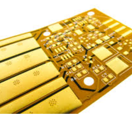
Unlike their rigid counterparts, flex PCBs are made from flexible materials such as polyimide, which allows them to bend and twist without breaking. This flexibility introduces unique design challenges, such as managing stress points and ensuring reliable electrical connections. Altium Designer provides a robust set of tools to address these challenges, making it a preferred choice for many engineers.
The first step in designing a flex PCB in Altium is to set up the project correctly.
This involves defining the board shape and layer stackup, which are crucial for ensuring that the final product meets the desired specifications. Altium allows designers to create complex layer stackups, including rigid-flex configurations, where both rigid and flexible sections are integrated into a single board. This capability is particularly useful for applications requiring both flexibility and structural support.
Once the project setup is complete, the next step is to design the circuit layout.
In this phase, it is important to consider the mechanical constraints of the flex PCB. For instance, traces should be routed in a manner that minimizes stress during bending. Altium’s design rule checks can be configured to flag potential issues, such as traces that are too close to bend areas or vias placed inappropriately. Additionally, using curved traces instead of sharp angles can help distribute stress more evenly, reducing the risk of trace cracking.
Transitioning to the component placement stage, designers must ensure that components are strategically placed to avoid areas of high mechanical stress.
Altium’s 3D visualization tools are invaluable in this regard, allowing designers to simulate how the board will bend and identify potential problem areas. This feature helps in optimizing component placement and ensuring that solder joints remain intact during flexing.
As the design progresses, it is crucial to perform thorough simulations and analyses to validate the board’s performance.
Altium offers a range of simulation tools that can be used to assess signal integrity, thermal performance, and mechanical durability. These simulations help identify potential issues early in the design process, reducing the likelihood of costly revisions later on.
Finally, once the design is complete, it is essential to generate accurate manufacturing outputs.
Altium’s comprehensive output generation capabilities ensure that all necessary files, such as Gerber files and assembly drawings, are correctly produced. This step is vital for ensuring that the manufacturer can accurately fabricate the flex PCB according to the design specifications.
In conclusion, designing flex PCBs in Altium requires a careful balance of electrical and mechanical considerations. By leveraging Altium’s advanced design tools and adhering to best practices, engineers can create reliable and innovative flex PCBs that meet the demands of modern electronic applications. As technology continues to evolve, the ability to design flexible circuits will remain a valuable skill in the electronics industry.
Best Practices for Flex PCB Layout in Altium
Designing flexible printed circuit boards (PCBs) in Altium Designer requires a meticulous approach to ensure both functionality and reliability. Flex PCBs, known for their ability to bend and conform to various shapes, are increasingly used in compact and dynamic electronic applications. To achieve optimal results, adhering to best practices during the layout process is essential.
Firstly, understanding the unique properties of flex PCBs is crucial. Unlike rigid PCBs, flex circuits are designed to withstand mechanical stress and bending.
Therefore, it is important to consider the material properties and the intended application environment. Altium Designer offers a range of tools to simulate and visualize the flexing behavior, which can be invaluable in the early stages of design.
When beginning the layout process, one should prioritize the stack-up configuration.
The stack-up defines the arrangement of conductive and insulating layers, which directly impacts the board’s flexibility and performance. In Altium, designers can utilize the Layer Stack Manager to configure and visualize the stack-up, ensuring that the flex layers are appropriately defined. It is advisable to use fewer layers to enhance flexibility, but this must be balanced with the electrical requirements of the design.
Routing is another critical aspect of flex PCB design.
To minimize stress on the traces, it is recommended to use curved traces instead of sharp angles. Altium’s advanced routing tools allow designers to create smooth, curved paths that reduce the risk of trace cracking during flexing. Additionally, maintaining consistent trace widths and spacing is vital to prevent impedance mismatches and signal integrity issues.
Transitioning from rigid to flex sections within a PCB requires careful attention.
The bend radius is a key parameter that dictates how tightly the board can be bent without damage. Altium provides design rules to specify minimum bend radii, which should be adhered to in order to avoid mechanical failure. Furthermore, it is beneficial to stagger vias and avoid placing them in bend areas, as they can act as stress concentrators.
Component placement on flex PCBs also demands strategic planning.
Components should be placed in areas that experience minimal bending to prevent mechanical stress on solder joints. Altium’s 3D visualization capabilities enable designers to assess component placement in relation to the board’s bending behavior, facilitating more informed decisions.
Thermal management is another consideration in flex PCB design.
The flexible materials used in these boards often have different thermal properties compared to rigid materials. Altium’s simulation tools can be used to analyze heat distribution and identify potential hotspots. Implementing thermal reliefs and ensuring adequate heat dissipation paths are effective strategies to manage thermal challenges.
Finally, thorough testing and validation are indispensable.
Altium Designer supports various simulation and analysis tools that allow for pre-fabrication testing of electrical and mechanical performance. By leveraging these tools, designers can identify and rectify potential issues before production, saving time and resources.
In conclusion, designing flex PCBs in Altium requires a comprehensive understanding of both the software’s capabilities and the unique demands of flexible circuits. By following best practices in stack-up configuration, routing, component placement, and thermal management, designers can create robust and reliable flex PCBs that meet the demands of modern electronic applications. Through careful planning and utilization of Altium’s advanced features, the challenges of flex PCB design can be effectively navigated, leading to successful project outcomes.
Overcoming Common Challenges in Flex PCB Design with Altium
Designing flexible printed circuit boards (PCBs) presents unique challenges that require careful consideration and specialized tools. Altium, a leading PCB design software, offers a suite of features that can help engineers overcome these challenges effectively.
One of the primary difficulties in flex PCB design is managing the mechanical properties of the board.
Unlike rigid PCBs, flex PCBs must withstand bending and flexing without compromising their electrical integrity. Altium addresses this by providing advanced simulation tools that allow designers to model the mechanical behavior of the board under various conditions. This capability enables engineers to predict potential failure points and make necessary adjustments before the manufacturing process begins.
Another common challenge in flex PCB design is the complexity of layer stack management.
Flex PCBs often require multiple layers, each with different materials and thicknesses, to achieve the desired flexibility and functionality. Altium simplifies this process with its intuitive layer stack manager, which allows designers to easily configure and visualize the stack-up of their boards. This feature not only streamlines the design process but also reduces the likelihood of errors that could lead to costly redesigns.
Signal integrity is another critical concern in flex PCB design.
The flexible nature of these boards can introduce issues such as signal distortion and electromagnetic interference. Altium’s comprehensive suite of signal integrity analysis tools helps designers identify and mitigate these issues early in the design phase. By simulating the electrical performance of the board, engineers can optimize trace routing and component placement to ensure reliable signal transmission.
Thermal management is also a significant consideration in flex PCB design.
The compact and flexible nature of these boards can lead to heat dissipation challenges, which, if not addressed, can affect the performance and longevity of the device. Altium provides thermal analysis tools that enable designers to assess the thermal performance of their designs and implement effective cooling strategies. This proactive approach helps prevent overheating and ensures the reliability of the final product.
Moreover, the integration of rigid and flexible sections within a single PCB, known as rigid-flex design, adds another layer of complexity.
Altium’s design environment supports rigid-flex design by allowing seamless transitions between rigid and flexible sections. This capability is crucial for applications that require both flexibility and structural support, such as wearable devices and medical implants. By facilitating the integration of these sections, Altium helps designers create more versatile and innovative products.
In addition to these technical challenges, flex PCB design often involves collaboration among multiple stakeholders, including electrical engineers, mechanical engineers, and manufacturers.
Altium’s collaborative design platform enables real-time communication and data sharing among team members, ensuring that everyone is aligned throughout the design process. This collaborative approach not only enhances efficiency but also reduces the risk of miscommunication and design errors.
In conclusion, while flex PCB design presents several challenges, Altium offers a comprehensive set of tools and features that help engineers navigate these complexities with confidence. From mechanical simulation and layer stack management to signal integrity analysis and thermal management, Altium provides the necessary resources to optimize flex PCB designs. By leveraging these capabilities, designers can overcome common obstacles and deliver high-quality, reliable products that meet the demands of today’s dynamic technology landscape.
Advanced Features in Altium for Flex PCB Prototyping
In the rapidly evolving field of electronics design, the demand for flexible printed circuit boards (PCBs) has surged, driven by the need for compact, lightweight, and versatile electronic devices. Altium Designer, a leading PCB design software, offers a suite of advanced features tailored specifically for flex PCB prototyping, enabling engineers to push the boundaries of innovation. Understanding these features is crucial for designers aiming to leverage the full potential of flex PCBs.
To begin with, Altium Designer provides a comprehensive set of tools for creating and managing the unique geometries associated with flex PCBs.
Unlike traditional rigid PCBs, flex circuits can bend and fold, necessitating a design approach that accommodates these dynamic movements. Altium’s layer stack manager is particularly beneficial in this regard, allowing designers to define and manipulate multiple stack layers, including rigid-flex combinations. This capability ensures that the mechanical and electrical properties of the flex PCB are optimized for the intended application.
Moreover, Altium Designer’s 3D visualization tools play a pivotal role in flex PCB prototyping.
These tools enable designers to visualize the board in a three-dimensional space, providing a realistic representation of how the flex PCB will behave in its operational environment. This feature is invaluable for identifying potential design issues, such as component interference or inadequate bend radius, before the prototyping phase. By simulating the physical behavior of the flex PCB, designers can make informed decisions that enhance the reliability and performance of the final product.
Transitioning from design to fabrication, Altium Designer offers robust support for generating the necessary documentation for flex PCB manufacturing.
The software’s design rule checks (DRC) are tailored to address the specific challenges of flex circuits, such as minimum bend radius and material constraints. These checks ensure that the design adheres to industry standards and manufacturing capabilities, reducing the risk of costly errors during production. Additionally, Altium’s output job files streamline the process of generating fabrication and assembly drawings, ensuring that all stakeholders have access to accurate and up-to-date information.
Another noteworthy feature of Altium Designer is its integration with various simulation tools, which is essential for validating the electrical performance of flex PCBs.
Signal integrity and power integrity analyses are critical for ensuring that the flex circuit functions as intended, particularly in high-speed and high-frequency applications. Altium’s simulation capabilities allow designers to model and analyze these parameters, providing insights into potential issues such as signal distortion or power loss. By addressing these concerns early in the design process, engineers can avoid costly redesigns and ensure that the final product meets performance expectations.
Furthermore, Altium Designer’s collaboration features facilitate seamless communication between design teams, which is particularly important in complex projects involving flex PCBs.
The software’s cloud-based platform allows multiple users to work on the same project simultaneously, ensuring that changes are tracked and documented in real-time. This collaborative approach not only enhances efficiency but also fosters innovation by enabling cross-disciplinary teams to contribute their expertise to the design process.
In conclusion, Altium Designer’s advanced features for flex PCB prototyping provide a comprehensive solution for engineers seeking to innovate in the field of flexible electronics. From design and visualization to simulation and collaboration, Altium equips designers with the tools necessary to navigate the complexities of flex PCB design, ultimately leading to the development of cutting-edge electronic devices. As the demand for flexible electronics continues to grow, mastering these features will be essential for staying competitive in the ever-evolving landscape of PCB design.