Flex pcb assembly process
Understanding The Basics Of Flex PCB Assembly
The flex PCB assembly process is a sophisticated and intricate procedure that plays a crucial role in the manufacturing of flexible printed circuit boards, which are essential components in modern electronic devices. Understanding the basics of this process is vital for those involved in electronics manufacturing, as it ensures the production of reliable and high-quality products.
To begin with, it is important to recognize that flex PCBs are distinct from their rigid counterparts due to their ability to bend and conform to various shapes.
This flexibility is achieved through the use of flexible substrates, such as polyimide, which provide the necessary pliability while maintaining electrical integrity.
The assembly process of flex PCBs involves several key stages, each of which requires meticulous attention to detail. Initially, the design phase is critical, as it sets the foundation for the entire assembly process. During this stage, engineers must carefully consider the layout and routing of the circuit, taking into account the unique properties of the flexible substrate. This involves using specialized design software that can accommodate the dynamic nature of flex PCBs, ensuring that the final product meets the desired specifications.
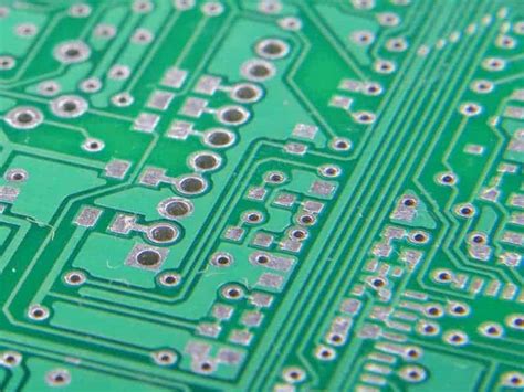
Following the design phase, the manufacturing process begins with the fabrication of the flex PCB.
This involves the creation of the circuit pattern on the flexible substrate through a series of steps, including photolithography, etching, and plating. These processes are similar to those used in the production of rigid PCBs, but they must be adapted to accommodate the flexible nature of the substrate. For instance, the etching process must be carefully controlled to prevent damage to the delicate material, while the plating process must ensure adequate adhesion of the conductive layers.
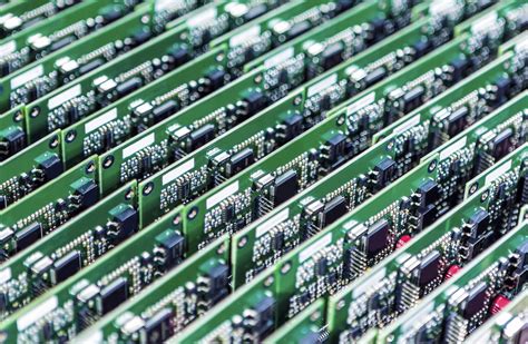
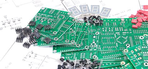
Once the flex PCB has been fabricated, the next step is the assembly of components onto the board.
This stage is particularly challenging due to the inherent flexibility of the substrate, which can complicate the placement and soldering of components. To address this, specialized equipment and techniques are employed, such as automated pick-and-place machines and reflow soldering processes that are specifically designed for flex PCBs. These tools help ensure precise component placement and reliable solder joints, which are essential for the functionality and durability of the final product.
Moreover, quality control is a critical aspect of the flex PCB assembly process.
Given the complexity and precision required, thorough testing and inspection are necessary to identify and rectify any defects or inconsistencies. This typically involves a combination of visual inspections, electrical testing, and advanced imaging techniques, such as X-ray or automated optical inspection (AOI), to verify the integrity of the assembly.
In conclusion, the flex PCB assembly process is a multifaceted procedure that demands a deep understanding of both the materials and techniques involved. By carefully navigating each stage of the process, from design and fabrication to assembly and quality control, manufacturers can produce high-quality flex PCBs that meet the rigorous demands of modern electronic applications. As technology continues to evolve, the importance of mastering the flex PCB assembly process will only grow, underscoring the need for ongoing innovation and expertise in this critical field.
Key Challenges In Flex PCB Assembly And How To Overcome Them
The flex PCB assembly process, while offering numerous advantages such as lightweight design and flexibility, presents a unique set of challenges that manufacturers must address to ensure optimal performance and reliability.
One of the primary challenges in flex PCB assembly is the inherent fragility of the flexible substrates.
Unlike rigid PCBs, flex PCBs are made from materials like polyimide, which, although durable, are more susceptible to damage during handling and assembly. To overcome this, manufacturers must implement stringent handling protocols and use specialized equipment designed to minimize stress on the flexible materials.
Another significant challenge is the alignment and registration of the layers.
Flex PCBs often involve multiple layers that need precise alignment to function correctly. Misalignment can lead to circuit failures and reduced performance. To address this, manufacturers can employ advanced imaging and alignment systems that ensure each layer is accurately positioned before bonding. Additionally, using fiducial markers on the PCB can aid in achieving precise alignment during the assembly process.
Soldering is another area where challenges frequently arise.
The thermal properties of flexible substrates differ from those of rigid boards, which can lead to issues such as warping or delamination during soldering. To mitigate these risks, manufacturers can use low-temperature soldering techniques and carefully control the thermal profiles during the soldering process. Moreover, selecting the appropriate solder paste and flux can help in achieving reliable solder joints without compromising the integrity of the flexible substrate.
Component placement on flex PCBs also poses unique challenges.
The flexibility of the substrate can lead to movement during component placement, resulting in misalignment or poor solder joint formation. To counter this, manufacturers can use fixtures or carriers that hold the flex PCB in place during assembly, ensuring stability and precision. Additionally, employing automated pick-and-place machines with vision systems can enhance accuracy in component placement.
Furthermore, testing and inspection of flex PCBs require specialized approaches.
Traditional testing methods may not be suitable due to the flexible nature of the boards. Manufacturers can adopt non-contact testing techniques, such as automated optical inspection (AOI) and X-ray inspection, to identify defects without exerting stress on the PCB. These methods allow for thorough inspection while preserving the integrity of the flexible substrate.
Finally, the design of flex PCBs can itself present challenges that impact the assembly process.
Complex designs with intricate trace patterns and tight tolerances can be difficult to manufacture and assemble. To overcome these challenges, collaboration between design and manufacturing teams is crucial. By involving manufacturing experts early in the design phase, potential issues can be identified and addressed before they become problematic during assembly. Design for manufacturability (DFM) principles can be applied to ensure that the PCB design is optimized for the assembly process, reducing the likelihood of defects and improving overall yield.
In conclusion, while the flex PCB assembly process presents several challenges, these can be effectively managed through careful planning, the use of advanced technologies, and close collaboration between design and manufacturing teams. By addressing these challenges head-on, manufacturers can harness the benefits of flex PCBs, delivering innovative and reliable solutions that meet the demands of modern electronic applications.
Innovations In Flex PCB Assembly Techniques
The field of electronics has witnessed significant advancements over the years, with flexible printed circuit boards (PCBs) emerging as a pivotal innovation. These flexible PCBs have revolutionized the way electronic devices are designed and manufactured, offering unparalleled versatility and adaptability. As the demand for more compact and efficient electronic devices continues to grow, the assembly techniques for flex PCBs have also evolved, incorporating cutting-edge technologies and methodologies to enhance performance and reliability.
One of the most notable innovations in flex PCB assembly is the development of advanced materials that improve flexibility and durability.
Traditional rigid PCBs are limited by their inability to bend or flex, which restricts their application in modern, compact devices. In contrast, flex PCBs are constructed using materials such as polyimide or polyester, which provide the necessary flexibility while maintaining electrical integrity. These materials not only allow for more intricate designs but also enable the creation of devices that can withstand mechanical stress and environmental factors, such as temperature fluctuations and moisture.
In addition to material advancements, the assembly process itself has seen significant improvements.
Surface mount technology (SMT) has become a cornerstone in flex PCB assembly, allowing for the placement of smaller and more complex components onto the flexible substrate. This technique enhances the overall functionality of the PCB by enabling higher component density and reducing the size of the final product. Moreover, SMT facilitates automated assembly processes, which increase production efficiency and reduce the likelihood of human error.
Furthermore, the integration of automated optical inspection (AOI) systems in the assembly process has greatly improved the quality control of flex PCBs.
AOI systems use high-resolution cameras and sophisticated algorithms to detect defects in the assembly, such as misaligned components or soldering issues. By identifying these defects early in the production process, manufacturers can ensure that only high-quality products reach the market, thereby reducing waste and enhancing customer satisfaction.
Another significant innovation in flex PCB assembly is the use of laser technology for cutting and drilling.
Traditional mechanical methods can cause stress and damage to the flexible substrate, potentially compromising the integrity of the PCB. Laser technology, on the other hand, offers a non-contact method that precisely cuts and drills the substrate without causing physical damage. This precision is particularly beneficial for complex designs that require intricate patterns and fine details.
Moreover, the advent of 3D printing technology has opened new possibilities in the assembly of flex PCBs.
3D printing allows for the creation of complex, multi-layered designs that were previously difficult to achieve with conventional methods. This technology not only speeds up the prototyping process but also enables the production of customized PCBs tailored to specific applications. As a result, manufacturers can quickly adapt to changing market demands and offer innovative solutions to their customers.
In conclusion, the innovations in flex PCB assembly techniques have significantly contributed to the advancement of electronic devices. Through the development of advanced materials, the adoption of surface mount technology, the integration of automated inspection systems, the use of laser technology, and the exploration of 3D printing, the assembly process has become more efficient, precise, and adaptable. As technology continues to evolve, it is expected that these innovations will further enhance the capabilities of flex PCBs, paving the way for even more sophisticated and versatile electronic devices in the future.
Quality Control Measures In Flex PCB Assembly Process
In the realm of electronics manufacturing, the flex PCB assembly process stands out for its complexity and precision. Ensuring the quality of flexible printed circuit boards (PCBs) is paramount, as these components are integral to a wide array of applications, from consumer electronics to aerospace technology. Consequently, implementing rigorous quality control measures is essential to guarantee the reliability and performance of the final product.
To begin with, the quality control process in flex PCB assembly starts with the selection of materials.
The choice of substrate, copper foil, and adhesive materials must meet stringent specifications to withstand the mechanical and thermal stresses encountered during operation. By conducting thorough material inspections and testing, manufacturers can prevent defects that may arise from substandard materials. This initial step is crucial, as it lays the foundation for the subsequent stages of assembly.
Following material selection, the focus shifts to the fabrication process, where precision is key.
During this phase, advanced imaging and etching techniques are employed to create the circuit patterns on the flexible substrate. To ensure accuracy, manufacturers utilize automated optical inspection (AOI) systems, which detect any discrepancies in the circuit patterns. These systems are capable of identifying minute defects that may not be visible to the naked eye, thus preventing potential failures in the final product.
As the assembly process progresses, soldering becomes a critical step that requires meticulous attention.
The use of surface mount technology (SMT) in flex PCB assembly necessitates precise control over solder paste application and reflow soldering temperatures. To achieve this, manufacturers employ X-ray inspection systems to verify the integrity of solder joints, ensuring that they are free from voids and misalignments. This non-destructive testing method provides a comprehensive view of the soldered connections, allowing for immediate corrective actions if necessary.
Moreover, electrical testing is an indispensable component of quality control in flex PCB assembly.
By conducting in-circuit testing (ICT) and functional testing, manufacturers can verify the electrical performance of the assembled PCBs. These tests assess parameters such as resistance, capacitance, and signal integrity, ensuring that the boards meet the required specifications. Through these rigorous evaluations, any deviations from the expected performance can be identified and rectified before the product reaches the end user.
In addition to these technical measures, maintaining a clean and controlled manufacturing environment is vital for ensuring quality.
Contaminants such as dust and moisture can adversely affect the performance of flex PCBs. Therefore, manufacturers implement strict environmental controls, including cleanroom facilities and humidity regulation, to minimize the risk of contamination. By maintaining a pristine production environment, the likelihood of defects is significantly reduced.
Furthermore, continuous improvement practices play a pivotal role in enhancing the quality control process.
By analyzing data from previous production runs and incorporating feedback from testing, manufacturers can identify trends and implement corrective actions to prevent recurring issues. This proactive approach not only improves the quality of the current production but also contributes to the development of more robust processes for future assemblies.
In conclusion, the quality control measures in the flex PCB assembly process are multifaceted and require a comprehensive approach. From material selection to environmental controls, each step is meticulously monitored to ensure the highest standards of quality. By employing advanced inspection technologies and adhering to stringent testing protocols, manufacturers can deliver reliable and high-performance flex PCBs that meet the demands of today’s sophisticated electronic applications.


