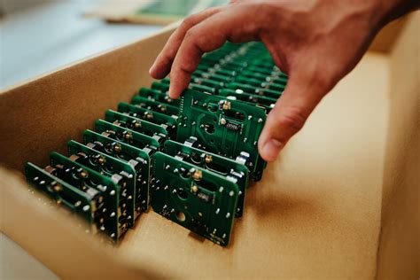
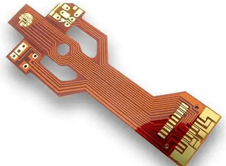
Flex pcb for camera module
Advantages Of Using Flex PCBs In Camera Modules
Flex PCBs, or flexible printed circuit boards, have become increasingly integral in the design and functionality of modern camera modules. Their unique properties offer a range of advantages that enhance the performance and versatility of camera systems.
One of the primary benefits of using flex PCBs in camera modules is their ability to conform to complex shapes and fit into compact spaces.
This flexibility allows for innovative camera designs that are not possible with traditional rigid PCBs. As camera modules continue to shrink in size, the demand for components that can adapt to limited space without compromising functionality has grown. Flex PCBs meet this demand by providing a solution that is both space-efficient and reliable.
In addition to their adaptability, flex PCBs contribute to the reduction of weight in camera modules.
This is particularly advantageous in applications where weight is a critical factor, such as in drones, mobile devices, and wearable technology. By minimizing the weight of the camera module, flex PCBs help improve the overall performance and user experience of these devices. Furthermore, the lightweight nature of flex PCBs does not come at the expense of durability. They are designed to withstand mechanical stress and environmental factors, making them suitable for use in a variety of challenging conditions.
Another significant advantage of flex PCBs is their ability to improve signal integrity within camera modules.
The flexible nature of these circuits allows for shorter and more direct routing of electrical signals, which reduces the potential for interference and signal loss. This is crucial in camera modules, where high-quality image capture and processing are dependent on the efficient transmission of data. By enhancing signal integrity, flex PCBs contribute to the production of clearer and more accurate images, which is essential for both consumer and professional-grade cameras.
Moreover, the use of flex PCBs in camera modules can lead to cost savings in the manufacturing process.
Their ability to integrate multiple components into a single assembly reduces the need for additional connectors and interconnects, which can be both costly and time-consuming to install. This integration not only simplifies the assembly process but also enhances the reliability of the camera module by reducing potential points of failure. As a result, manufacturers can produce high-quality camera modules more efficiently and at a lower cost, which can be passed on to consumers in the form of more affordable products.
In addition to these practical benefits, flex PCBs also offer design flexibility that encourages innovation in camera technology.
Engineers and designers can experiment with new configurations and layouts that were previously unattainable with rigid PCBs. This freedom to explore new design possibilities can lead to the development of advanced camera features and capabilities, further pushing the boundaries of what is possible in imaging technology.
In conclusion, the advantages of using flex PCBs in camera modules are manifold.
Their adaptability, lightweight nature, improved signal integrity, cost-effectiveness, and design flexibility make them an ideal choice for modern camera systems. As technology continues to evolve, the role of flex PCBs in enhancing the functionality and performance of camera modules is likely to become even more pronounced, driving further innovation in the field of imaging technology.
Design Considerations For Flex PCBs In Camera Applications
In the rapidly evolving world of electronics, the integration of flexible printed circuit boards (flex PCBs) into camera modules has become increasingly prevalent. This trend is driven by the demand for compact, lightweight, and versatile electronic devices. Flex PCBs offer a unique set of advantages that make them particularly suitable for camera applications, but their design requires careful consideration to ensure optimal performance and reliability.
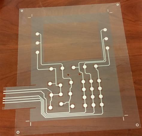
To begin with, one of the primary benefits of using flex PCBs in camera modules is their ability to conform to complex shapes and fit into tight spaces.
This flexibility allows for more innovative and compact camera designs, which is particularly important in applications such as smartphones, drones, and wearable devices. However, this very flexibility necessitates a thorough understanding of the mechanical stresses that the PCB will encounter during its lifecycle. Designers must account for bending, twisting, and other dynamic movements that could potentially lead to mechanical failure or signal integrity issues.
Moreover, the choice of materials is a critical factor in the design of flex PCBs for camera modules.
The substrate material must be carefully selected to balance flexibility with durability. Polyimide is a popular choice due to its excellent thermal stability and mechanical properties. However, the specific requirements of the camera application, such as operating temperature range and exposure to environmental factors, may necessitate the use of alternative materials or additional protective coatings.
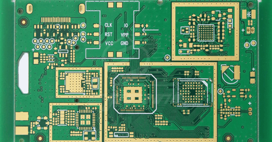
In addition to material selection, the layout of the flex PCB is another crucial consideration.
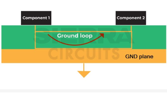
The routing of traces must be meticulously planned to minimize electromagnetic interference (EMI) and ensure signal integrity. This is particularly important in camera modules, where high-speed data transmission is often required. Designers must also consider the placement of components to optimize space utilization while maintaining the necessary electrical connections. The use of blind and buried vias can help achieve a more compact design, but they also add complexity to the manufacturing process.
Thermal management is another key aspect of flex PCB design in camera applications.
Camera modules can generate significant amounts of heat, which must be effectively dissipated to prevent damage to sensitive components. The use of thermal vias, heat sinks, and other cooling techniques can help manage heat dissipation. Additionally, the choice of materials with good thermal conductivity can aid in maintaining a stable operating temperature.
Furthermore, the reliability of flex PCBs in camera modules is paramount, given the critical nature of their applications.
Rigorous testing and validation processes are essential to ensure that the flex PCB can withstand the environmental and operational stresses it will encounter. This includes testing for thermal cycling, mechanical fatigue, and exposure to moisture and other environmental factors.
In conclusion, the design of flex PCBs for camera applications involves a complex interplay of factors, including mechanical flexibility, material selection, layout optimization, thermal management, and reliability testing. By carefully considering these aspects, designers can create flex PCBs that not only meet the demanding requirements of modern camera modules but also contribute to the development of more innovative and compact electronic devices. As technology continues to advance, the role of flex PCBs in camera applications is likely to expand, offering new opportunities and challenges for designers in this dynamic field.
Manufacturing Challenges Of Flex PCBs For Camera Modules
The manufacturing of flexible printed circuit boards (flex PCBs) for camera modules presents a unique set of challenges that require careful consideration and innovative solutions. As the demand for compact and high-performance camera modules increases, particularly in smartphones and other portable devices, the role of flex PCBs becomes increasingly critical. These components must not only accommodate the intricate circuitry required for advanced camera functions but also maintain flexibility and durability under various conditions.
One of the primary challenges in manufacturing flex PCBs for camera modules is the need for miniaturization.
As devices become smaller, the space available for components like camera modules is significantly reduced. This necessitates the development of flex PCBs that can support high-density interconnections while maintaining a minimal footprint. Achieving this requires advanced fabrication techniques and materials that can support fine line widths and tight tolerances. The use of advanced photolithography and etching processes is essential to create the intricate patterns required for these high-density circuits.
In addition to miniaturization, the mechanical flexibility of the PCB is a crucial factor.
Camera modules often need to be positioned at various angles within a device, requiring the PCB to bend and flex without compromising its electrical integrity. This demands the use of materials that can withstand repeated flexing without cracking or losing conductivity. Polyimide films are commonly used in flex PCBs due to their excellent thermal stability and mechanical properties. However, ensuring consistent performance across different batches of material can be challenging, necessitating rigorous quality control measures.
Thermal management is another significant challenge in the manufacturing of flex PCBs for camera modules.
As camera modules become more sophisticated, they generate more heat, which can affect the performance and reliability of the PCB. Effective thermal management solutions, such as the integration of heat sinks or the use of thermally conductive materials, are essential to dissipate heat efficiently. This requires a careful balance between maintaining the flexibility of the PCB and enhancing its thermal properties.
Moreover, the integration of additional components, such as sensors and lenses, onto the flex PCB adds another layer of complexity.
These components must be precisely aligned and securely attached to ensure optimal performance. The use of advanced assembly techniques, such as surface mount technology (SMT) and automated optical inspection (AOI), is crucial to achieve the high level of precision required. Additionally, the adhesive materials used in the assembly process must be carefully selected to ensure they do not interfere with the electrical performance or flexibility of the PCB.
Finally, the environmental conditions in which camera modules operate can pose challenges for flex PCB manufacturing
. These modules are often exposed to varying temperatures, humidity levels, and mechanical stresses, all of which can impact the performance and longevity of the PCB. To address these challenges, manufacturers must conduct extensive testing and validation to ensure that the flex PCBs can withstand these conditions without degradation.
In conclusion, the manufacturing of flex PCBs for camera modules involves navigating a complex landscape of challenges, from miniaturization and mechanical flexibility to thermal management and environmental resilience. By leveraging advanced materials, fabrication techniques, and assembly processes, manufacturers can overcome these challenges and produce high-quality flex PCBs that meet the demanding requirements of modern camera modules. As technology continues to evolve, ongoing innovation and adaptation will be essential to address the ever-changing needs of this dynamic industry.
Innovations In Flex PCB Technology For Camera Systems
In recent years, the evolution of flexible printed circuit boards (flex PCBs) has significantly impacted the design and functionality of camera systems. As the demand for compact, lightweight, and high-performance cameras continues to grow, particularly in consumer electronics, automotive, and industrial applications, flex PCBs have emerged as a pivotal technology. These innovative circuit boards offer a range of benefits that enhance the capabilities of camera modules, making them indispensable in modern imaging solutions.
One of the primary advantages of flex PCBs in camera systems is their ability to accommodate complex designs in limited spaces.
Unlike traditional rigid PCBs, flex PCBs can be bent, folded, and twisted to fit into the intricate and compact structures of camera modules. This flexibility allows for more efficient use of space, enabling manufacturers to design smaller and lighter cameras without compromising on performance. Consequently, this has led to the development of ultra-compact cameras that are now ubiquitous in smartphones, drones, and wearable devices.
Moreover, flex PCBs contribute to improved reliability and durability in camera systems.
The flexible nature of these circuit boards allows them to absorb mechanical stresses and vibrations more effectively than their rigid counterparts. This is particularly beneficial in applications where cameras are subject to constant movement or harsh environmental conditions, such as in automotive or industrial settings. By reducing the risk of damage from physical stress, flex PCBs help ensure the longevity and consistent performance of camera modules.
In addition to their mechanical advantages, flex PCBs also offer superior electrical performance.
They can support high-density interconnections and complex circuitry, which are essential for advanced camera functionalities such as high-resolution imaging, rapid autofocus, and image stabilization. The ability to integrate multiple components on a single flex PCB reduces the need for additional connectors and wiring, thereby minimizing signal loss and enhancing overall system efficiency. This integration capability is crucial for meeting the increasing demands for higher data transfer rates and improved image processing in modern camera systems.
Furthermore, the use of flex PCBs in camera modules facilitates greater design flexibility and innovation.
Engineers can experiment with various configurations and layouts, leading to the development of novel camera designs that were previously unattainable with rigid PCBs. This has opened up new possibilities in the design of panoramic cameras, 360-degree cameras, and other specialized imaging devices that require unique form factors and functionalities.
As the technology continues to advance, the integration of flex PCBs with other emerging technologies is expected to drive further innovations in camera systems.
For instance, the combination of flex PCBs with advanced materials such as conductive polymers and nanomaterials could lead to even more compact and efficient camera modules. Additionally, the integration of flex PCBs with wireless communication technologies could enable the development of smart cameras with enhanced connectivity and remote control capabilities.
In conclusion, the innovations in flex PCB technology have revolutionized the design and functionality of camera systems, offering numerous advantages in terms of space efficiency, reliability, electrical performance, and design flexibility. As the demand for advanced imaging solutions continues to rise, the role of flex PCBs in camera modules is likely to become even more significant, paving the way for the next generation of high-performance, compact, and versatile cameras.