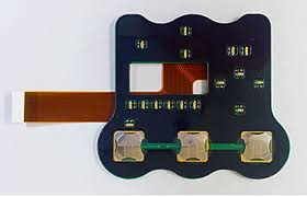
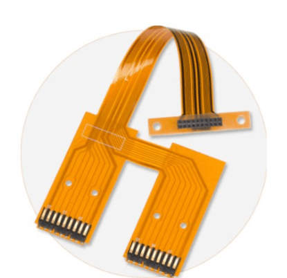
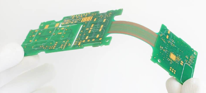
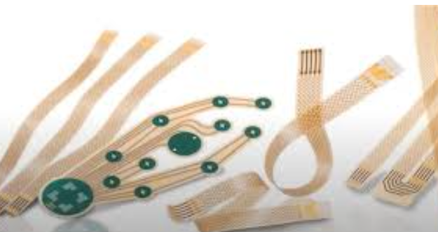
Flex pcb fpc
Advantages Of Flex PCB FPC In Modern Electronics
Flex PCBs, or flexible printed circuit boards, have become a cornerstone in the evolution of modern electronics, offering a multitude of advantages that cater to the ever-growing demand for compact, efficient, and reliable electronic devices. As technology continues to advance, the need for components that can adapt to various shapes and spaces has become increasingly important. Flex PCBs, also known as FPCs, provide a solution to this need by offering unparalleled flexibility and versatility in design and application.
One of the primary advantages of flex PCBs is their ability to conform to complex geometries.
Unlike traditional rigid PCBs, flex PCBs can be bent, folded, and twisted without compromising their functionality. This adaptability allows for innovative product designs, enabling manufacturers to create smaller, lighter, and more efficient devices. For instance, in the realm of consumer electronics, flex PCBs are integral to the development of wearable technology, where space is limited and the need for flexibility is paramount. By utilizing flex PCBs, designers can maximize the use of available space, leading to more compact and ergonomic products.
In addition to their physical flexibility, flex PCBs offer significant improvements in terms of reliability and durability.
The materials used in flex PCBs, such as polyimide, are known for their excellent thermal stability and resistance to environmental stressors. This makes them ideal for applications that require high reliability under challenging conditions, such as automotive and aerospace industries. The inherent resilience of flex PCBs reduces the risk of failure due to mechanical stress, vibration, or thermal expansion, thereby enhancing the overall longevity and performance of electronic devices.
Moreover, flex PCBs contribute to cost efficiency in manufacturing processes.
Their ability to reduce the number of interconnects and connectors needed in a circuit design simplifies assembly and minimizes potential points of failure. This not only streamlines production but also reduces the likelihood of defects, leading to lower production costs and improved yield rates. Furthermore, the lightweight nature of flex PCBs can result in reduced shipping and handling costs, providing additional economic benefits to manufacturers.
Another noteworthy advantage of flex PCBs is their capacity to support high-density circuit designs.
As electronic devices become more sophisticated, the demand for increased functionality within a limited space grows. Flex PCBs can accommodate complex circuitry and multiple layers, allowing for the integration of more components without increasing the size of the board. This capability is particularly beneficial in the development of advanced technologies such as smartphones, tablets, and medical devices, where space is at a premium and performance cannot be compromised.
In conclusion, the advantages of flex PCBs in modern electronics are manifold, encompassing flexibility, reliability, cost efficiency, and support for high-density designs. As the electronics industry continues to push the boundaries of innovation, the role of flex PCBs is set to become even more pivotal. By enabling the creation of smaller, more efficient, and more reliable devices, flex PCBs are not only meeting the current demands of the market but are also paving the way for future technological advancements. As such, their importance in the landscape of modern electronics cannot be overstated, making them an indispensable component in the pursuit of cutting-edge solutions.
Design Considerations For Flex PCB FPC Applications
When designing flexible printed circuit boards (FPCs), several critical considerations must be taken into account to ensure optimal performance and reliability. Flex PCBs, known for their ability to bend and conform to various shapes, are increasingly used in applications where space constraints and mechanical flexibility are paramount. As such, understanding the unique design requirements of FPCs is essential for engineers and designers aiming to leverage their full potential.
To begin with, material selection plays a pivotal role in the design of flex PCBs.
The choice of substrate material, typically polyimide, is crucial due to its excellent thermal stability and flexibility. Polyimide’s ability to withstand high temperatures and its inherent flexibility make it an ideal choice for applications that require repeated bending or exposure to harsh environments. Additionally, the copper used for the conductive traces must be carefully selected to balance flexibility with electrical performance. Thinner copper layers are often preferred to enhance flexibility, but they must be thick enough to handle the required current loads without excessive resistance.
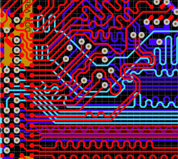
Transitioning to the layout design, it is important to consider the bend radius of the flex PCB.
The bend radius is the minimum radius that the board can be bent without causing damage to the conductive traces or the substrate. A larger bend radius reduces the risk of mechanical stress and potential failure, thus enhancing the durability of the FPC. Designers must also account for the dynamic flexing requirements of the application, ensuring that the board can withstand repeated bending cycles without degradation.
Moreover, trace routing is another critical aspect of FPC design.
To minimize stress on the traces during bending, it is advisable to route them perpendicular to the bend line rather than parallel. This routing strategy helps distribute mechanical stress more evenly across the traces, reducing the likelihood of cracking or delamination. Additionally, incorporating teardrop patterns at the junctions where traces meet pads can further enhance mechanical strength and reliability.
In terms of component placement, designers should be mindful of the areas that will experience the most flexing.
Placing components in regions that undergo frequent bending can lead to mechanical fatigue and eventual failure. Therefore, it is recommended to position components in static areas of the board, away from the primary bend zones. If components must be placed in flexing areas, using flexible adhesive or encapsulation materials can help mitigate stress and protect the components.
Thermal management is another consideration that cannot be overlooked.
Flex PCBs, due to their thin and flexible nature, may have limited heat dissipation capabilities. Therefore, designers must ensure that adequate thermal management solutions are in place, such as thermal vias or heat sinks, to prevent overheating and ensure reliable operation.
Finally, the choice of connectors and interconnects is crucial for maintaining signal integrity and mechanical stability.
Flexible connectors that can accommodate the movement of the FPC without compromising electrical connections are essential. Additionally, ensuring proper strain relief at the connector interface can prevent mechanical stress from being transferred to the solder joints, thereby enhancing the overall reliability of the assembly.
In conclusion, designing flex PCBs requires a comprehensive understanding of the unique challenges and considerations associated with their use. By carefully selecting materials, optimizing layout and routing, and addressing thermal and mechanical concerns, designers can create robust and reliable FPCs that meet the demands of modern electronic applications.
Manufacturing Process Of Flex PCB FPC
The manufacturing process of Flex PCB (Flexible Printed Circuit Board) FPC is a sophisticated and intricate procedure that requires precision and expertise. This process begins with the selection of appropriate materials, which is crucial for ensuring the flexibility and durability of the final product. Typically, polyimide is chosen as the substrate material due to its excellent thermal stability and flexibility. The copper foil, which serves as the conductive layer, is laminated onto the polyimide substrate. This lamination process is performed under controlled conditions to ensure a strong bond between the layers.
Once the materials are prepared, the next step involves the application of a photoresist layer onto the copper foil.
This photoresist is a light-sensitive material that plays a critical role in the subsequent photolithography process. During photolithography, the photoresist-coated copper is exposed to ultraviolet light through a photomask, which contains the desired circuit pattern. The exposure to light causes the photoresist to harden in the areas where the circuit pattern is present, while the unexposed areas remain soft and can be easily removed.
Following the photolithography process, the board undergoes an etching process.
In this step, a chemical solution is used to remove the unwanted copper, leaving behind only the copper traces that form the circuit pattern. The precision of this etching process is vital, as it directly affects the performance and reliability of the Flex PCB FPC. After etching, the remaining photoresist is stripped away, revealing the clean copper traces.
Subsequently, the board is subjected to a series of cleaning processes to remove any residual chemicals and contaminants.
This ensures that the surface is pristine and ready for the next stages of manufacturing. At this point, additional layers, such as coverlays or solder masks, may be applied to protect the copper traces and enhance the board’s durability. These layers are typically made from flexible materials that do not compromise the board’s flexibility.
The next phase involves drilling holes for vias and mounting points.
These holes are essential for establishing electrical connections between different layers of the board and for attaching components. The drilling process must be executed with high precision to maintain the integrity of the board and ensure reliable connections.
Once the drilling is complete, the board undergoes a plating process.
This involves depositing a thin layer of metal, usually copper, onto the walls of the drilled holes to create conductive pathways. The plating process is followed by a series of inspections and tests to verify the board’s electrical performance and structural integrity.
Finally, the Flex PCB FPC is cut into its final shape and size.
This cutting process, often performed using laser technology, ensures clean edges and precise dimensions. The finished boards are then subjected to rigorous quality control checks to ensure they meet the required specifications and standards.
In conclusion, the manufacturing process of Flex PCB FPC is a complex sequence of steps that demands meticulous attention to detail and adherence to stringent quality standards. Each stage, from material selection to final inspection, plays a crucial role in producing a flexible circuit board that meets the demands of modern electronic applications. Through this intricate process, manufacturers are able to deliver high-quality Flex PCBs that are essential for a wide range of industries, including consumer electronics, automotive, and medical devices.
Future Trends In Flex PCB FPC Technology
The realm of flexible printed circuit boards (FPCs) is witnessing a transformative evolution, driven by the relentless pursuit of innovation and the increasing demand for miniaturized, efficient, and versatile electronic solutions. As technology continues to advance at an unprecedented pace, the future trends in flex PCB FPC technology are poised to redefine the landscape of electronic design and manufacturing.
One of the most significant trends is the integration of advanced materials that enhance the performance and durability of FPCs.
Researchers and manufacturers are exploring novel substrates and conductive materials that offer superior flexibility, thermal stability, and electrical conductivity. These materials not only improve the reliability of FPCs in demanding applications but also enable the development of thinner and lighter circuits, which are crucial for modern electronic devices.
In addition to material advancements, the miniaturization of electronic components is a key trend shaping the future of flex PCB FPC technology.
As consumer electronics, medical devices, and wearable technologies continue to shrink in size, the demand for compact and efficient circuit solutions is on the rise. Flexible PCBs are uniquely positioned to meet this demand, as they can be designed to fit into unconventional shapes and spaces, providing designers with unparalleled freedom and creativity. This trend is further accelerated by the development of advanced manufacturing techniques, such as laser direct structuring and additive manufacturing, which allow for precise and intricate circuit designs that were previously unattainable.
Moreover, the growing emphasis on sustainability and environmental responsibility is influencing the direction of flex PCB FPC technology.
Manufacturers are increasingly adopting eco-friendly practices and materials to reduce the environmental impact of their products. This includes the use of recyclable substrates, lead-free soldering processes, and energy-efficient manufacturing techniques. As regulatory pressures and consumer awareness continue to mount, the adoption of sustainable practices in FPC production is expected to become a standard rather than an exception.
Another promising trend is the integration of flexible PCBs with emerging technologies such as the Internet of Things (IoT) and 5G connectivity.
The inherent flexibility and adaptability of FPCs make them ideal for IoT applications, where devices often require seamless integration into everyday objects and environments. As 5G networks expand, the demand for high-speed, low-latency communication solutions will drive the development of FPCs that can support these advanced connectivity requirements. This convergence of technologies is likely to result in a new generation of smart devices that are more interconnected and capable than ever before.
Furthermore, the rise of artificial intelligence (AI) and machine learning is expected to have a profound impact on the design and functionality of flexible PCBs.
AI-driven design tools are enabling engineers to optimize circuit layouts and performance with unprecedented precision, leading to more efficient and reliable FPCs. Additionally, the integration of AI capabilities into flexible circuits could pave the way for intelligent systems that can adapt and respond to their environment in real-time, opening up new possibilities for applications in healthcare, automotive, and consumer electronics.
In conclusion, the future trends in flex PCB FPC technology are characterized by a confluence of material innovation, miniaturization, sustainability, and integration with emerging technologies. As these trends continue to evolve, they will undoubtedly shape the future of electronics, offering new opportunities and challenges for designers, manufacturers, and consumers alike. The ongoing advancements in this field promise to deliver more efficient, versatile, and sustainable electronic solutions that will drive the next wave of technological innovation.