Flex pcb gerber
Introduction To Flex PCB Gerber Files
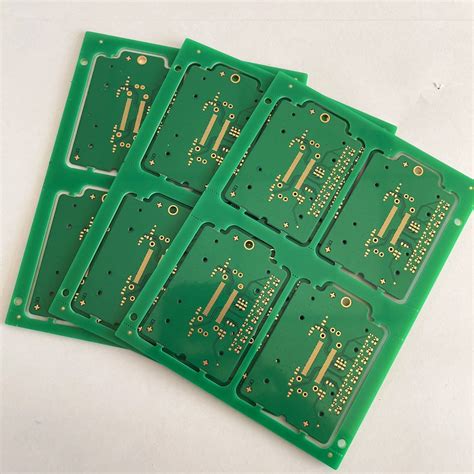
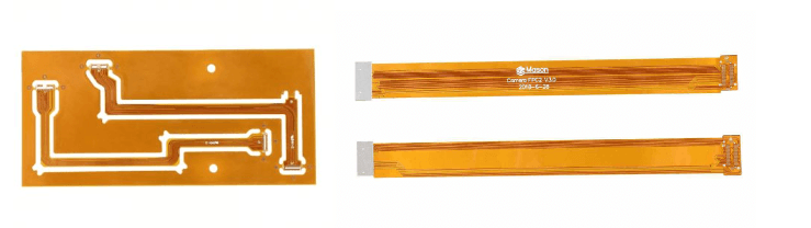
Flex PCB Gerber files are an essential component in the design and manufacturing of flexible printed circuit boards (PCBs).
These files serve as the blueprint for the production process, providing detailed information about the various layers and features of the PCB. Understanding the intricacies of Flex PCB Gerber files is crucial for engineers and designers who aim to create reliable and efficient flexible circuits.
To begin with, it is important to recognize that Gerber files are a standard format used in the PCB industry to describe the layout of a circuit board.
These files contain data on the copper layers, solder mask, silkscreen, and other essential elements. In the context of flexible PCBs, Gerber files play a pivotal role in ensuring that the unique properties of flexible materials are accurately represented and adhered to during manufacturing.
One of the primary distinctions between rigid and flexible PCBs lies in the materials used.
Flexible PCBs are typically made from polyimide or other flexible substrates, which allow the board to bend and flex without breaking. This flexibility is advantageous in applications where space constraints and mechanical stress are significant considerations. Consequently, the Gerber files for flex PCBs must account for these material properties, ensuring that the design can withstand the intended mechanical movements and stresses.
Moreover, the process of creating Flex PCB Gerber files involves several critical steps.
Initially, the design is created using specialized PCB design software. This software allows designers to define the various layers, trace widths, and other parameters essential for the circuit’s functionality. Once the design is complete, the software generates the Gerber files, which are then reviewed and verified for accuracy. This verification process is crucial, as any errors in the Gerber files can lead to costly manufacturing defects and delays.
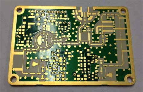
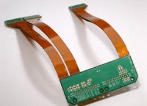
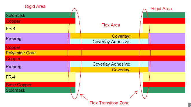
In addition to the standard layers found in rigid PCBs, flex PCBs often include additional layers such as coverlays and stiffeners.
Coverlays are used to protect the flexible circuits from environmental factors and mechanical damage, while stiffeners provide additional support in areas where components are mounted. The Gerber files must accurately represent these additional layers, ensuring that they are correctly integrated into the final design.
Furthermore, the manufacturing process for flexible PCBs requires specialized equipment and techniques.
The Gerber files guide this process, providing precise instructions for each step. For instance, the files dictate the patterning of the copper layers, the application of the coverlay, and the placement of components. By following the Gerber files, manufacturers can produce flexible PCBs that meet the stringent requirements of various applications, from consumer electronics to medical devices.
It is also worth noting that advancements in technology have led to the development of more sophisticated PCB design tools and software.
These tools offer enhanced capabilities for creating and managing Flex PCB Gerber files, making the design process more efficient and accurate. As a result, designers can now create more complex and reliable flexible circuits, pushing the boundaries of what is possible in electronic design.
In conclusion, Flex PCB Gerber files are a fundamental aspect of the design and manufacturing process for flexible printed circuit boards. They provide a detailed blueprint that ensures the accurate representation of the circuit’s layout and features. By understanding the importance of these files and the steps involved in their creation, engineers and designers can produce high-quality flexible PCBs that meet the demands of modern electronic applications.
Designing Flex PCBs: Best Practices For Gerber Files
In the realm of modern electronics, flexible printed circuit boards (Flex PCBs) have emerged as a pivotal innovation, offering unparalleled versatility and adaptability. As the demand for compact, lightweight, and flexible electronic devices continues to surge, the importance of meticulously designing Flex PCBs cannot be overstated. Central to this design process is the creation of Gerber files, which serve as the blueprint for manufacturing these intricate circuits. To ensure the successful production of Flex PCBs, adhering to best practices in Gerber file design is essential.
To begin with, understanding the unique characteristics of Flex PCBs is crucial.
Unlike their rigid counterparts, Flex PCBs are designed to bend and twist, accommodating complex geometries and dynamic applications. This inherent flexibility necessitates a careful consideration of material properties, layer stack-ups, and trace routing. Consequently, when generating Gerber files, it is imperative to account for these factors to prevent mechanical failures and ensure optimal performance.
One of the fundamental aspects of designing Flex PCBs is the selection of appropriate materials.
Polyimide is a commonly used substrate due to its excellent thermal stability and mechanical properties. However, the choice of adhesive and coverlay materials also plays a significant role in the overall durability and flexibility of the PCB. When creating Gerber files, specifying these materials accurately is vital to avoid discrepancies during the manufacturing process.
Transitioning to the layout design, trace routing demands meticulous attention.
In Flex PCBs, traces are more susceptible to mechanical stress, which can lead to cracking or delamination. To mitigate these risks, designers should employ curved traces instead of sharp angles, as this reduces stress concentration points. Additionally, maintaining consistent trace widths and spacing is essential to ensure uniform current distribution and minimize the risk of electrical failures. These considerations should be clearly reflected in the Gerber files to guide the fabrication process accurately.
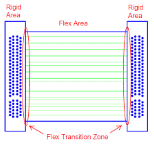
Another critical aspect is the layer stack-up configuration.
Flex PCBs often incorporate multiple layers to achieve the desired functionality while maintaining flexibility. Properly defining the layer stack-up in the Gerber files is paramount to avoid misalignment and ensure precise layer registration during manufacturing. Furthermore, incorporating stiffeners in strategic locations can enhance the mechanical stability of the PCB without compromising its flexibility. These stiffeners should be clearly indicated in the Gerber files to facilitate accurate assembly.
Moreover, the inclusion of design for manufacturability (DFM) guidelines in the Gerber files can significantly streamline the production process.
DFM guidelines encompass various aspects such as minimum trace widths, spacing, hole sizes, and tolerances. By adhering to these guidelines, designers can minimize the risk of manufacturing defects and ensure a higher yield. Communicating these guidelines effectively through the Gerber files is essential to align the design intent with the capabilities of the manufacturing process.
In addition to the technical considerations, thorough documentation is indispensable.
Gerber files should be accompanied by comprehensive fabrication notes, including details on material specifications, layer stack-up, trace routing guidelines, and any special instructions. This documentation serves as a vital reference for manufacturers, ensuring that the final product aligns with the design intent.
In conclusion, designing Flex PCBs necessitates a meticulous approach to Gerber file creation. By understanding the unique characteristics of Flex PCBs, selecting appropriate materials, optimizing trace routing, defining layer stack-ups accurately, adhering to DFM guidelines, and providing thorough documentation, designers can ensure the successful production of high-quality Flex PCBs. As the demand for flexible electronics continues to grow, mastering these best practices will be instrumental in advancing the capabilities and applications of Flex PCBs in the ever-evolving landscape of modern technology.
Common Mistakes In Flex PCB Gerber File Creation
Creating a Flex PCB Gerber file is a meticulous process that requires precision and attention to detail. However, even experienced designers can make mistakes that can lead to costly errors and delays in production. One common mistake is the improper handling of layer stack-ups. Flex PCBs often involve multiple layers, and any misalignment or incorrect sequencing can result in a non-functional board. It is crucial to ensure that each layer is correctly defined and aligned in the Gerber file to avoid such issues.
Another frequent error is the incorrect specification of material properties.
Flex PCBs use different materials compared to rigid PCBs, and these materials have unique properties that must be accurately represented in the Gerber file. Failing to specify the correct material properties can lead to issues such as improper bending, cracking, or even complete failure of the PCB. Therefore, it is essential to consult material datasheets and ensure that all relevant properties are correctly included in the design files.
Designers also often overlook the importance of proper trace width and spacing.
Flex PCBs are more susceptible to mechanical stress, and inadequate trace width or spacing can lead to broken connections or short circuits. It is vital to follow industry standards and guidelines for trace width and spacing to ensure the reliability and durability of the final product. Additionally, using advanced design rules and simulation tools can help identify potential issues early in the design process.
Another area where mistakes commonly occur is in the creation of drill files.
Flex PCBs often require precise hole placements for components and vias. Any errors in the drill file can result in misaligned holes, which can cause assembly issues or even render the PCB unusable. It is important to double-check all drill file specifications and ensure that they match the design requirements.
Furthermore, designers sometimes neglect to include necessary documentation and notes in the Gerber file.
Flex PCBs often have unique requirements and constraints that need to be communicated to the manufacturer. Including detailed notes and documentation can help avoid misunderstandings and ensure that the PCB is manufactured correctly. This includes specifying bend areas, stiffener locations, and any special handling instructions.
Another common mistake is the improper use of design software. Many designers use software tools that are not specifically tailored for flex PCB design, leading to errors and inefficiencies. It is advisable to use specialized software that can handle the unique requirements of flex PCBs, such as bend radius calculations and material property simulations. This can help streamline the design process and reduce the likelihood of errors.
Lastly, inadequate testing and verification can lead to significant issues in the final product.
It is essential to thoroughly test and verify the Gerber file before sending it to manufacturing. This includes running design rule checks, performing simulations, and conducting prototype testing. By identifying and addressing potential issues early, designers can avoid costly rework and ensure a successful final product.
In conclusion, creating a Flex PCB Gerber file involves several critical steps that require careful attention to detail. By avoiding common mistakes such as improper layer stack-ups, incorrect material specifications, inadequate trace width and spacing, errors in drill files, lack of documentation, improper use of design software, and insufficient testing, designers can ensure a smooth and successful manufacturing process. Taking the time to meticulously review and verify the Gerber file can save time, reduce costs, and result in a high-quality flex PCB.
Advanced Techniques For Optimizing Flex PCB Gerber Files
Flex PCB Gerber files are essential in the design and manufacturing of flexible printed circuit boards, which are increasingly prevalent in modern electronics due to their versatility and space-saving properties. Optimizing these files is crucial for ensuring the efficiency, reliability, and cost-effectiveness of the final product. Advanced techniques for optimizing Flex PCB Gerber files involve a combination of design best practices, meticulous attention to detail, and leveraging specialized software tools.
To begin with, one of the fundamental aspects of optimizing Flex PCB Gerber files is ensuring that the design adheres to the specific requirements of flexible circuits.
Unlike rigid PCBs, flex PCBs must accommodate bending and flexing without compromising the integrity of the electrical connections. Therefore, it is imperative to use appropriate materials and layer stack-ups that can withstand mechanical stress. Additionally, incorporating curved traces instead of sharp angles can significantly reduce the risk of cracking and improve the overall durability of the flex PCB.
Another critical technique involves the strategic placement of components and vias.
In flex PCB design, it is essential to avoid placing components and vias in areas that will experience significant bending. This precaution helps prevent mechanical stress on solder joints and vias, which can lead to failures. Instead, these elements should be positioned in stable regions of the PCB, where they are less likely to be affected by flexing. Furthermore, using teardrop-shaped pads for vias and component leads can enhance the mechanical strength and reliability of the connections.
Signal integrity is another vital consideration when optimizing Flex PCB Gerber files.
High-speed signals can be particularly challenging to manage in flexible circuits due to the potential for signal degradation and electromagnetic interference. To mitigate these issues, designers should carefully route high-speed traces, ensuring that they are kept as short and direct as possible. Additionally, maintaining consistent trace widths and spacing, as well as using controlled impedance techniques, can help preserve signal integrity. Shielding and grounding strategies, such as incorporating ground planes and using differential pairs, are also effective in minimizing interference and crosstalk.
Thermal management is another crucial aspect of flex PCB optimization.
Flexible circuits can be more susceptible to thermal stress due to their thinner and more pliable nature. To address this, designers should consider the thermal properties of the materials used and ensure adequate heat dissipation. This can be achieved by incorporating thermal vias, heat sinks, and appropriate copper thicknesses. Additionally, spreading out heat-generating components and avoiding high-density areas can help distribute heat more evenly across the PCB.
Leveraging advanced software tools is also instrumental in optimizing Flex PCB Gerber files.
Modern PCB design software offers a range of features specifically tailored for flexible circuits, such as bend simulation, dynamic design rule checks, and automated trace routing. These tools can help identify potential issues early in the design process, allowing for timely adjustments and refinements. Moreover, using 3D visualization capabilities can provide a more comprehensive understanding of how the flex PCB will behave in its final application, facilitating better design decisions.
In conclusion, optimizing Flex PCB Gerber files requires a multifaceted approach that encompasses material selection, component placement, signal integrity, thermal management, and the use of advanced design tools. By adhering to these advanced techniques, designers can create flexible circuits that are not only reliable and efficient but also cost-effective and well-suited to the demands of modern electronic applications.