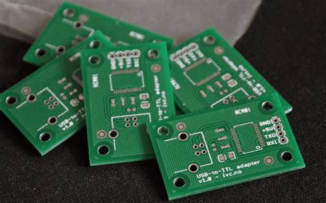
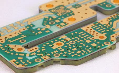
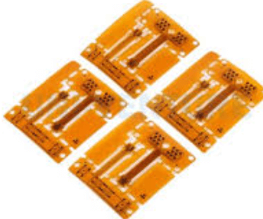
Flex pcb impedance
Understanding Flex PCB Impedance: Key Factors and Considerations
Understanding Flex PCB Impedance: Key Factors and Considerations
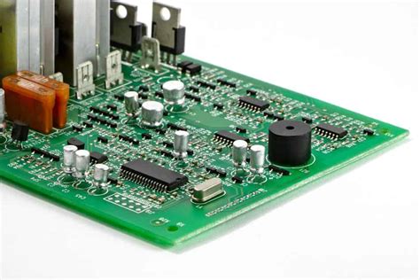
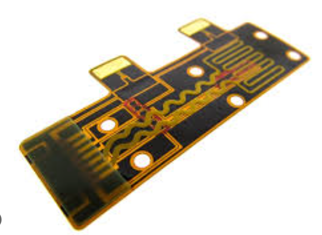
Flex PCBs, or flexible printed circuit boards, have become increasingly prevalent in modern electronics due to their versatility, lightweight nature, and ability to conform to various shapes. However, one critical aspect that engineers must consider when designing flex PCBs is impedance. Impedance, the measure of opposition that a circuit presents to the flow of alternating current, plays a crucial role in ensuring signal integrity and overall performance. Understanding the key factors and considerations related to flex PCB impedance is essential for achieving optimal functionality.
To begin with, the material properties of the flex PCB significantly influence impedance.
Flex PCBs are typically made from polyimide or polyester substrates, which have different dielectric constants. The dielectric constant, a measure of a material’s ability to store electrical energy in an electric field, affects the impedance of the circuit. A higher dielectric constant results in lower impedance, while a lower dielectric constant leads to higher impedance. Therefore, selecting the appropriate substrate material based on the desired impedance characteristics is a fundamental step in the design process.
Moreover, the geometry of the traces on the flex PCB is another critical factor.
The width, thickness, and spacing of the traces directly impact the impedance. For instance, wider traces tend to have lower impedance, while narrower traces exhibit higher impedance. Similarly, the thickness of the copper layer used for the traces also affects impedance; thicker copper layers reduce impedance, whereas thinner layers increase it. Additionally, the spacing between traces, known as the pitch, plays a role in determining impedance. Closer spacing results in higher impedance, while wider spacing lowers it. Consequently, careful consideration of trace geometry is necessary to achieve the desired impedance values.
Transitioning to the next consideration, the environment in which the flex PCB operates can also affect impedance.
Factors such as temperature, humidity, and mechanical stress can alter the material properties and geometry of the flex PCB, thereby impacting impedance. For example, temperature variations can cause the substrate material to expand or contract, leading to changes in the dielectric constant and trace dimensions. Similarly, mechanical stress from bending or flexing the PCB can deform the traces, affecting their width and spacing. Therefore, it is crucial to account for the operating environment and design the flex PCB to maintain stable impedance under varying conditions.
Furthermore, the frequency of the signals transmitted through the flex PCB is a vital consideration.
Impedance is frequency-dependent, meaning that it varies with the frequency of the alternating current. At higher frequencies, the skin effect becomes more pronounced, causing the current to concentrate near the surface of the traces. This phenomenon increases the effective resistance and inductance of the traces, thereby altering the impedance. Consequently, designing flex PCBs for high-frequency applications requires careful analysis and optimization of impedance to ensure signal integrity.
In addition to these factors, the use of controlled impedance techniques is essential for achieving precise impedance values.
Controlled impedance involves designing the flex PCB with specific trace geometries and materials to achieve a target impedance. This process often requires simulation and modeling tools to predict and fine-tune the impedance characteristics accurately. By employing controlled impedance techniques, engineers can ensure that the flex PCB meets the required impedance specifications, thereby enhancing performance and reliability.
In conclusion, understanding and managing flex PCB impedance is crucial for optimizing the performance of modern electronic devices. By considering factors such as material properties, trace geometry, operating environment, signal frequency, and employing controlled impedance techniques, engineers can design flex PCBs that maintain stable and precise impedance values. This, in turn, ensures signal integrity, reduces electromagnetic interference, and enhances the overall functionality of the electronic system.
Designing for Controlled Impedance in Flexible PCBs
Designing for controlled impedance in flexible printed circuit boards (PCBs) is a critical aspect of modern electronics engineering, particularly as devices become more compact and their performance requirements more stringent. Controlled impedance ensures that the signal integrity is maintained across the PCB, which is essential for high-speed digital and RF applications. To achieve this, several factors must be considered during the design phase, including material selection, trace geometry, and the overall layout of the PCB.
Firstly, the choice of materials plays a pivotal role in determining the impedance characteristics of a flexible PCB.
The dielectric constant (Dk) and dissipation factor (Df) of the substrate material directly influence the impedance. Materials such as polyimide and liquid crystal polymer (LCP) are commonly used due to their favorable electrical properties and flexibility. These materials provide a stable dielectric constant over a wide frequency range, which is crucial for maintaining consistent impedance.
In addition to material selection, the geometry of the traces is another significant factor.
The width and thickness of the copper traces, as well as the spacing between them, must be precisely controlled. For instance, wider traces will have lower impedance, while narrower traces will have higher impedance. Similarly, the thickness of the copper layer affects the impedance; thicker layers reduce impedance, whereas thinner layers increase it. Therefore, careful calculation and simulation are required to determine the optimal trace dimensions that meet the desired impedance specifications.
Moreover, the layout of the flexible PCB must be meticulously planned to ensure controlled impedance.
This involves considering the stack-up configuration, which includes the arrangement of signal and ground layers. A common practice is to use a microstrip or stripline configuration, where the signal trace is either on the outer layer with a ground plane beneath it (microstrip) or sandwiched between two ground planes (stripline). These configurations help to confine the electromagnetic fields and reduce signal loss, thereby maintaining the desired impedance.
Furthermore, the bending and flexing nature of flexible PCBs introduces additional challenges in maintaining controlled impedance.
The mechanical stress from bending can alter the trace geometry and the dielectric properties of the substrate, potentially affecting the impedance. To mitigate these effects, designers often incorporate features such as curved traces and strain reliefs, which distribute the mechanical stress more evenly and reduce the risk of impedance variation.
Additionally, advanced simulation tools are indispensable in the design process for controlled impedance in flexible PCBs.
These tools allow designers to model the electrical behavior of the PCB under various conditions, including different frequencies and bending scenarios. By simulating the impedance characteristics, designers can make informed decisions about material selection, trace geometry, and layout, ensuring that the final product meets the required specifications.
In conclusion, designing for controlled impedance in flexible PCBs is a multifaceted process that requires careful consideration of material properties, trace geometry, and layout configuration. By meticulously planning and utilizing advanced simulation tools, designers can achieve the desired impedance characteristics, ensuring signal integrity and optimal performance in high-speed and RF applications. As technology continues to advance, the importance of controlled impedance in flexible PCBs will only grow, making it an essential aspect of modern electronics design.

Common Challenges in Flex PCB Impedance Control and How to Overcome Them
Flex PCB impedance control is a critical aspect of designing flexible printed circuit boards, particularly in high-frequency applications where signal integrity is paramount. One of the common challenges in flex PCB impedance control is the variability in material properties. Unlike rigid PCBs, flex PCBs use materials such as polyimide, which can exhibit significant variations in dielectric constant and thickness. These variations can lead to inconsistencies in impedance, making it difficult to achieve the desired electrical performance. To overcome this challenge, it is essential to work closely with material suppliers to ensure that the materials used have tightly controlled properties. Additionally, conducting thorough material characterization and implementing robust design rules can help mitigate the impact of material variability on impedance control.
Another challenge in flex PCB impedance control is the complexity of the stack-up design.
Flex PCBs often require multiple layers and intricate geometries to accommodate the bending and flexing requirements of the application. This complexity can make it difficult to maintain consistent impedance across the entire board. To address this issue, designers should use advanced simulation tools to model the impedance of the entire stack-up accurately. These tools can help identify potential problem areas and allow for adjustments to be made before the board is fabricated. Furthermore, working with experienced PCB manufacturers who have expertise in flex PCB design can provide valuable insights and recommendations for optimizing the stack-up design.
The manufacturing process itself can also introduce challenges in flex PCB impedance control.
Factors such as etching precision, layer alignment, and adhesive application can all impact the final impedance of the board. To minimize these effects, it is crucial to select a manufacturer with a proven track record of producing high-quality flex PCBs. Implementing stringent quality control measures throughout the manufacturing process, including regular inspections and testing, can help ensure that the final product meets the desired impedance specifications. Additionally, collaborating with the manufacturer during the design phase can help identify potential manufacturing challenges early on and allow for design adjustments to be made accordingly.
Environmental factors can also pose challenges to flex PCB impedance control.
Flex PCBs are often used in applications where they are exposed to varying temperatures, humidity levels, and mechanical stresses. These environmental conditions can affect the dielectric properties of the materials and, consequently, the impedance of the board. To mitigate these effects, it is important to select materials that are specifically designed for the intended operating environment. Conducting environmental testing during the design phase can also help identify potential issues and allow for design modifications to be made to ensure reliable performance under varying conditions.
In conclusion, achieving precise impedance control in flex PCBs involves addressing several challenges related to material properties, stack-up design, manufacturing processes, and environmental factors. By working closely with material suppliers, using advanced simulation tools, selecting experienced manufacturers, and conducting thorough testing, designers can overcome these challenges and ensure that their flex PCBs meet the required impedance specifications. This approach not only enhances the performance and reliability of the final product but also helps avoid costly redesigns and delays in the development process.
The Role of Material Selection in Flex PCB Impedance Management
In the realm of flexible printed circuit boards (PCBs), impedance management is a critical factor that significantly influences the performance and reliability of electronic devices. One of the most pivotal aspects of impedance control in flex PCBs is the selection of materials. The choice of materials not only affects the electrical properties but also impacts the mechanical flexibility and durability of the circuit. Therefore, understanding the role of material selection in flex PCB impedance management is essential for engineers and designers aiming to optimize their designs.
To begin with, the dielectric constant (Dk) of the substrate material plays a crucial role in determining the impedance of a flex PCB.
The dielectric constant is a measure of a material’s ability to store electrical energy in an electric field. Materials with a high dielectric constant can lead to lower impedance, while those with a low dielectric constant result in higher impedance. Consequently, selecting a substrate material with an appropriate dielectric constant is fundamental to achieving the desired impedance levels. For instance, polyimide, a commonly used material in flex PCBs, has a relatively stable dielectric constant, making it a preferred choice for many applications.
In addition to the dielectric constant, the thickness of the substrate material also influences impedance.
Thicker substrates generally result in lower impedance, whereas thinner substrates lead to higher impedance. This relationship necessitates careful consideration of the substrate thickness during the design phase. Engineers must balance the need for mechanical flexibility with the electrical requirements of the circuit. For example, in applications where space constraints are critical, a thinner substrate may be necessary, but this choice must be counterbalanced by adjustments in other design parameters to maintain the desired impedance.
Moreover, the type of conductive material used in the flex PCB is another significant factor in impedance management.
Copper is the most commonly used conductive material due to its excellent electrical conductivity and flexibility. However, the thickness and width of the copper traces can affect the impedance. Thicker and wider traces typically result in lower impedance, while thinner and narrower traces lead to higher impedance. Therefore, precise control over the dimensions of the copper traces is essential to ensure consistent impedance throughout the circuit.
Furthermore, the adhesive materials used in flex PCBs can also impact impedance.
Adhesives are used to bond the various layers of the PCB together, and their dielectric properties can influence the overall impedance of the circuit. Selecting adhesives with suitable dielectric properties is crucial to maintaining the desired impedance levels. Additionally, the uniformity and consistency of the adhesive application are important to avoid variations in impedance that could affect the performance of the circuit.
Transitioning to the environmental considerations, the operating conditions of the flex PCB, such as temperature and humidity, can also affect impedance.
Materials that exhibit stable electrical properties under varying environmental conditions are preferred to ensure reliable performance. For instance, polyimide not only offers a stable dielectric constant but also demonstrates excellent thermal stability, making it suitable for applications subjected to high temperatures.
In conclusion, the selection of materials in flex PCBs is a multifaceted process that significantly impacts impedance management. By carefully considering the dielectric constant, substrate thickness, conductive material properties, adhesive characteristics, and environmental stability, engineers can optimize the impedance of flex PCBs to meet the specific requirements of their applications. This meticulous approach to material selection ensures that the final product delivers reliable and efficient performance, thereby enhancing the overall functionality of electronic devices.