Flex pcb impedance
Understanding Impedance Control in Flex PCBs
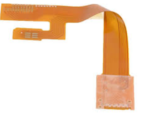
In the realm of modern electronics, the demand for flexible printed circuit boards (PCBs) has surged, driven by the need for compact, lightweight, and versatile electronic devices. A critical aspect of designing these flex PCBs is understanding and controlling impedance, which plays a pivotal role in ensuring signal integrity and overall device performance. Impedance, in the context of PCBs, refers to the opposition that a circuit presents to the flow of alternating current (AC) and is a function of the circuit’s resistance, inductance, and capacitance. As electronic devices become more sophisticated, the need for precise impedance control becomes increasingly important, particularly in high-frequency applications.
To begin with, impedance control in flex PCBs is essential for maintaining signal integrity, which is crucial for the reliable operation of high-speed digital and RF circuits.
When signals travel through a PCB, they encounter various materials and geometries that can cause reflections, signal loss, and distortion if the impedance is not properly managed. These issues can lead to data errors, reduced performance, and even device failure. Therefore, achieving the desired impedance is a fundamental design consideration for engineers working with flex PCBs.
The process of controlling impedance in flex PCBs involves several factors, including the choice of materials, the geometry of the traces, and the configuration of the layers.
Flex PCBs are typically made from polyimide or polyester substrates, which offer excellent flexibility and thermal stability. However, these materials have different dielectric constants, which affect the impedance of the traces. By carefully selecting the substrate material and its thickness, designers can influence the impedance characteristics of the PCB.
Moreover, the geometry of the traces, including their width, thickness, and spacing, plays a significant role in determining impedance.
For instance, wider traces tend to have lower impedance, while narrower traces have higher impedance. Additionally, the spacing between traces can affect crosstalk, which is the unwanted transfer of signals between adjacent traces. By optimizing trace geometry, designers can achieve the desired impedance while minimizing crosstalk and other signal integrity issues.
Layer configuration is another critical aspect of impedance control in flex PCBs.
Multilayer flex PCBs allow for more complex designs and can help manage impedance by providing additional ground and power planes. These planes serve as reference points for the signal traces, helping to stabilize impedance and reduce electromagnetic interference (EMI). By strategically placing these layers, designers can create controlled impedance environments that enhance signal integrity.
Furthermore, simulation and modeling tools are invaluable in the design process, allowing engineers to predict and adjust the impedance characteristics of flex PCBs before fabrication.
These tools enable the analysis of various design parameters and their impact on impedance, facilitating the optimization of the PCB layout for specific applications. By leveraging these technologies, designers can ensure that their flex PCBs meet the stringent requirements of modern electronic devices.
In conclusion, understanding and controlling impedance in flex PCBs is a complex but essential task that directly impacts the performance and reliability of electronic devices. By carefully considering material selection, trace geometry, and layer configuration, and utilizing advanced simulation tools, engineers can design flex PCBs that meet the demanding needs of today’s high-speed and high-frequency applications. As technology continues to evolve, the importance of impedance control in flex PCBs will only grow, underscoring its critical role in the future of electronics design.

Design Tips for Managing Impedance in Flexible Circuits
When designing flexible printed circuit boards (PCBs), managing impedance is a critical consideration that can significantly impact the performance and reliability of the final product. Flexible circuits, known for their ability to bend and conform to various shapes, are increasingly used in applications where space constraints and dynamic movement are factors. However, their unique properties also introduce challenges in maintaining consistent impedance, which is crucial for high-speed signal integrity.
To begin with, understanding the fundamental principles of impedance in flexible circuits is essential.
Impedance, in the context of PCBs, refers to the resistance a circuit offers to the flow of alternating current (AC). It is influenced by several factors, including the geometry of the traces, the dielectric material properties, and the frequency of the signals. In flexible circuits, the variability in these factors can be more pronounced due to the inherent flexibility and the materials used, such as polyimide substrates.
One of the primary design tips for managing impedance in flexible circuits is to carefully consider the trace width and spacing.
The trace width directly affects the impedance; wider traces typically result in lower impedance, while narrower traces increase it. Therefore, maintaining consistent trace widths is crucial, especially in areas where the circuit will bend or flex. Additionally, the spacing between traces should be optimized to minimize crosstalk and electromagnetic interference, which can further affect impedance.
Moreover, the choice of dielectric material plays a significant role in impedance control.
Flexible circuits often use materials like polyimide, which have different dielectric constants compared to rigid PCB materials. The dielectric constant affects the capacitance between the traces and the ground plane, thereby influencing the impedance. Selecting a dielectric material with a stable dielectric constant across the operating temperature range can help maintain consistent impedance.
Another important aspect is the stack-up configuration of the flexible circuit.
The stack-up refers to the arrangement of conductive and insulating layers within the PCB. In flexible circuits, the stack-up can be more complex due to the need for additional layers to provide mechanical support and flexibility. Designers should ensure that the stack-up is symmetrical and balanced to prevent warping and to maintain uniform impedance across the circuit.
Furthermore, the use of controlled impedance traces is a common practice in flexible circuit design.
Controlled impedance involves designing traces with specific dimensions and spacing to achieve a desired impedance value. This technique is particularly important for high-speed digital and RF applications, where signal integrity is paramount. By simulating the impedance during the design phase and making necessary adjustments, designers can ensure that the final product meets the required specifications.
In addition to these design considerations, it is also advisable to collaborate closely with the PCB manufacturer.
Manufacturers can provide valuable insights into the material properties and fabrication processes that can affect impedance. By working together, designers and manufacturers can identify potential issues early in the design process and implement solutions to mitigate them.
In conclusion, managing impedance in flexible circuits requires a comprehensive understanding of the factors that influence it and careful attention to design details. By optimizing trace geometry, selecting appropriate materials, configuring the stack-up effectively, and employing controlled impedance techniques, designers can achieve reliable and high-performance flexible circuits. As technology continues to advance, the demand for flexible PCBs will grow, making impedance management an increasingly important aspect of circuit design.
The Role of Material Selection in Flex PCB Impedance
In the realm of flexible printed circuit boards (flex PCBs), impedance control is a critical factor that significantly influences the performance and reliability of electronic devices. The role of material selection in determining flex PCB impedance cannot be overstated, as it directly impacts signal integrity, power distribution, and overall functionality. Understanding the interplay between material properties and impedance is essential for engineers and designers aiming to optimize their designs for high-frequency applications.
To begin with, the dielectric material used in flex PCBs plays a pivotal role in impedance control.
The dielectric constant, or relative permittivity, of the material affects the speed at which signals propagate through the circuit. Materials with a lower dielectric constant are generally preferred for high-speed applications, as they allow signals to travel faster and with less distortion. Polyimide is a commonly used dielectric material in flex PCBs due to its excellent thermal stability and mechanical flexibility. However, its relatively high dielectric constant can pose challenges for impedance control, necessitating careful consideration of other material properties and design parameters.
In addition to the dielectric constant, the thickness of the dielectric layer is another crucial factor influencing impedance.
Thicker dielectric layers can increase the characteristic impedance of a transmission line, which may be desirable or undesirable depending on the specific application. Designers must strike a balance between achieving the desired impedance and maintaining the flexibility and mechanical integrity of the PCB. This often involves selecting materials that offer a combination of low dielectric constant and appropriate thickness to meet the design requirements.
Furthermore, the choice of conductive materials also affects flex PCB impedance.
Copper is the most commonly used conductor in PCBs due to its excellent electrical conductivity and availability. However, the surface roughness of copper can introduce additional impedance variations, particularly at high frequencies. To mitigate this, manufacturers often employ techniques such as smoothening the copper surface or using alternative conductive materials with lower surface roughness. These measures help maintain consistent impedance levels across the PCB, ensuring reliable signal transmission.
Moreover, the adhesive materials used in flex PCBs can influence impedance characteristics.
Adhesives are typically employed to bond the various layers of the PCB together, and their dielectric properties can affect the overall impedance of the circuit. Selecting adhesives with low dielectric constants and minimal loss tangents is crucial for maintaining signal integrity, especially in high-frequency applications. Additionally, the thermal and mechanical properties of adhesives must be considered to ensure they can withstand the operating conditions of the device without compromising performance.
Transitioning to the design aspect, the layout and geometry of the traces on a flex PCB also play a significant role in impedance control.
The width, spacing, and routing of traces must be carefully designed to achieve the desired impedance levels. This often involves using simulation tools to model the impedance characteristics of different trace configurations and iterating on the design to optimize performance. By considering the interplay between material properties and trace design, engineers can achieve precise impedance control, which is essential for minimizing signal reflections and ensuring reliable data transmission.
In conclusion, material selection is a fundamental aspect of flex PCB design that directly impacts impedance control. By carefully choosing dielectric materials, conductive materials, adhesives, and trace configurations, designers can optimize the performance of flex PCBs for a wide range of applications. Understanding the complex relationship between these factors is essential for achieving the desired electrical characteristics and ensuring the reliability and efficiency of electronic devices.
Common Challenges in Flex PCB Impedance and How to Overcome Them
Flex PCB impedance is a critical factor in the design and functionality of flexible printed circuit boards, which are increasingly used in modern electronics due to their versatility and space-saving capabilities. However, achieving the desired impedance in flex PCBs presents several challenges that designers and engineers must address to ensure optimal performance. Understanding these challenges and implementing effective solutions is essential for the successful deployment of flex PCBs in various applications.
One of the primary challenges in managing flex PCB impedance is the variability in material properties.
Flex PCBs are typically made from polyimide or polyester substrates, which can exhibit different dielectric constants and loss tangents compared to traditional rigid PCB materials. This variability can lead to inconsistencies in impedance control, making it difficult to achieve the precise impedance values required for high-speed signal transmission. To overcome this challenge, it is crucial to select materials with well-characterized and consistent dielectric properties. Additionally, working closely with material suppliers to obtain detailed specifications and conducting thorough testing can help ensure that the chosen materials meet the necessary impedance requirements.
Another significant challenge is the impact of the flex PCB’s physical structure on impedance.
The flexible nature of these boards means that they can bend and twist, which can alter the geometry of the traces and, consequently, the impedance. This is particularly problematic in applications where the PCB is subject to frequent or extreme flexing. To mitigate this issue, designers can employ techniques such as using wider traces or incorporating ground planes to stabilize the impedance. Moreover, simulating the flexing behavior during the design phase can help identify potential impedance variations and allow for adjustments before manufacturing.
The manufacturing process itself can also introduce challenges in maintaining consistent impedance.
Variations in etching, lamination, and other fabrication steps can lead to discrepancies in trace width, thickness, and spacing, all of which affect impedance. To address these issues, it is essential to work with experienced manufacturers who have a proven track record in producing high-quality flex PCBs. Implementing stringent quality control measures and conducting regular inspections throughout the manufacturing process can further help ensure that the final product meets the desired impedance specifications.
In addition to these technical challenges, there are also design considerations that can impact flex PCB impedance.
For instance, the layout of the traces and the arrangement of components can influence the overall impedance of the circuit. Designers must carefully plan the routing of traces to minimize impedance discontinuities and avoid sharp bends or abrupt changes in trace width. Utilizing advanced design software that can simulate impedance and signal integrity can be invaluable in optimizing the layout and ensuring that the design meets the required specifications.
In conclusion, while managing flex PCB impedance presents several challenges, understanding the underlying factors and implementing strategic solutions can significantly enhance the performance and reliability of these versatile circuit boards. By selecting appropriate materials, considering the physical structure, ensuring precise manufacturing processes, and optimizing design layouts, engineers can effectively overcome the common challenges associated with flex PCB impedance. As technology continues to advance, the demand for flexible and reliable electronic solutions will only grow, making it increasingly important to address these challenges with diligence and expertise.

