Flex pcb panelization
Benefits Of Flex PCB Panelization In Modern Electronics
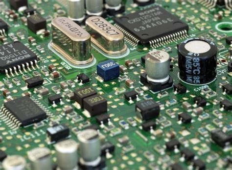
Flex PCB panelization has emerged as a pivotal technique in the realm of modern electronics, offering a multitude of benefits that enhance both the manufacturing process and the performance of electronic devices.
As the demand for smaller, more efficient, and versatile electronic products continues to rise, the role of flex PCB panelization becomes increasingly significant. This process involves grouping multiple flexible printed circuit boards (PCBs) onto a single panel, which is then processed as a unit. By doing so, manufacturers can achieve greater efficiency and cost-effectiveness, while also addressing the growing complexity of electronic designs.
One of the primary advantages of flex PCB panelization is the optimization of manufacturing efficiency.
By processing multiple circuits simultaneously, manufacturers can significantly reduce the time and labor required for production. This is particularly beneficial in high-volume manufacturing environments, where time savings can translate into substantial cost reductions. Moreover, panelization minimizes material waste, as the layout can be optimized to utilize the available space on the panel effectively. This not only conserves resources but also contributes to a more sustainable manufacturing process.
In addition to efficiency gains, flex PCB panelization enhances the reliability and performance of electronic devices
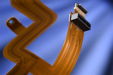
. The flexible nature of these PCBs allows for greater design versatility, enabling the creation of complex, three-dimensional circuit configurations that would be challenging or impossible with rigid PCBs. This flexibility is particularly advantageous in applications where space is limited, such as in wearable technology, medical devices, and compact consumer electronics. By allowing circuits to bend and conform to the contours of the device, flex PCBs can improve the overall functionality and user experience.
Furthermore, the panelization process facilitates better quality control and testing.
By handling multiple circuits as a single unit, manufacturers can implement more rigorous testing protocols, ensuring that each individual circuit meets the required standards before being separated from the panel. This comprehensive approach to quality assurance helps to reduce the likelihood of defects and failures in the final product, thereby enhancing the reliability and longevity of electronic devices.
Another noteworthy benefit of flex PCB panelization is its contribution to cost-effectiveness.
The ability to produce multiple circuits simultaneously reduces the per-unit cost of manufacturing, making it an attractive option for companies looking to optimize their production budgets. Additionally, the reduction in material waste and the streamlined assembly process further contribute to cost savings. These financial advantages are particularly important in a competitive market, where manufacturers are constantly seeking ways to deliver high-quality products at lower prices.
Moreover, flex PCB panelization supports the trend towards miniaturization in electronics.
As devices become smaller and more complex, the need for compact and efficient circuit solutions becomes paramount. Flex PCBs, with their ability to fit into tight spaces and accommodate intricate designs, are ideally suited to meet these demands. By enabling the production of smaller, lighter, and more efficient electronic components, panelization plays a crucial role in advancing the capabilities of modern technology.
In conclusion, flex PCB panelization offers a range of benefits that are essential to the advancement of modern electronics. From improving manufacturing efficiency and reducing costs to enhancing device performance and supporting miniaturization, this technique is integral to meeting the evolving demands of the industry. As technology continues to progress, the importance of flex PCB panelization is likely to grow, solidifying its role as a cornerstone of electronic manufacturing.
Techniques For Efficient Flex PCB Panelization
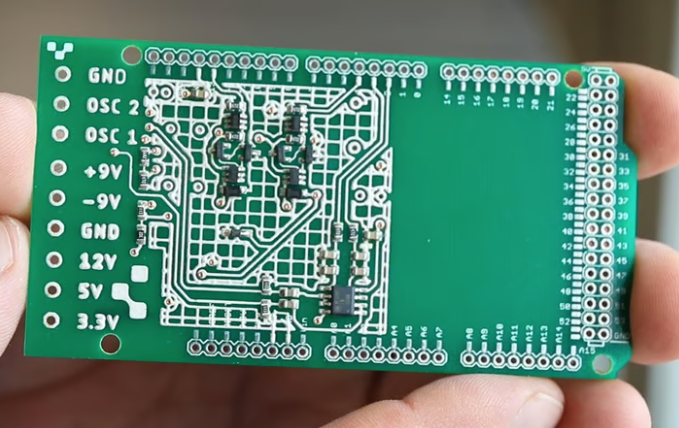
Flex PCB panelization is a crucial process in the manufacturing of flexible printed circuit boards, aimed at optimizing production efficiency and reducing costs. This technique involves arranging multiple individual PCBs on a single panel, allowing them to be processed simultaneously. As the demand for compact and lightweight electronic devices continues to grow, the importance of efficient flex PCB panelization cannot be overstated. By employing effective panelization strategies, manufacturers can enhance yield, minimize material waste, and streamline assembly processes.
One of the primary techniques for efficient flex PCB panelization is the use of a well-designed panel layout.
The layout should be optimized to maximize the number of PCBs per panel while ensuring that each board can be easily separated after manufacturing. This involves careful consideration of the board’s shape, size, and the spacing between individual units. By minimizing the distance between PCBs, manufacturers can reduce material waste and improve the overall efficiency of the production process. Additionally, a well-planned layout can facilitate automated assembly and testing, further enhancing productivity.
Another important aspect of flex PCB panelization is the choice of panelization method.
There are several methods available, each with its own advantages and limitations. The most common methods include V-scoring, tab-routing, and breakaway tabs. V-scoring involves making V-shaped cuts along the edges of the PCBs, allowing them to be easily snapped apart after assembly. This method is particularly suitable for simple board designs with straight edges.
On the other hand, tab-routing involves creating small tabs that connect the individual PCBs to the panel frame.
These tabs can be easily broken or routed out after manufacturing, making this method ideal for more complex board shapes. Breakaway tabs, similar to tab-routing, involve the use of perforated tabs that can be snapped off, providing a balance between ease of separation and structural integrity during assembly.
In addition to selecting the appropriate panelization method, manufacturers must also consider the material properties of the flex PCBs.
The flexibility and thinness of these boards present unique challenges during panelization. It is essential to ensure that the panelization process does not compromise the mechanical integrity of the boards. This can be achieved by using support materials, such as stiffeners or carriers, during the manufacturing process. These materials provide additional rigidity, preventing damage during handling and assembly.
Furthermore, the use of fiducial markers is a critical component of efficient flex PCB panelization.
Fiducial markers are reference points that aid in the alignment and positioning of the PCBs during assembly. By incorporating these markers into the panel design, manufacturers can ensure precise placement of components, reducing the risk of errors and improving overall yield. The strategic placement of fiducial markers can also facilitate automated optical inspection, enhancing quality control measures.
In conclusion, efficient flex PCB panelization is a multifaceted process that requires careful consideration of various factors, including panel layout, panelization method, material properties, and the use of fiducial markers. By optimizing these elements, manufacturers can achieve significant improvements in production efficiency, cost-effectiveness, and product quality. As the electronics industry continues to evolve, the importance of mastering flex PCB panelization techniques will only increase, making it a critical area of focus for manufacturers seeking to remain competitive in the market.
Challenges And Solutions In Flex PCB Panelization
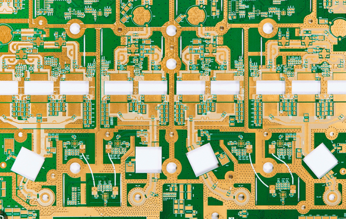
Flex PCB panelization, a critical process in the manufacturing of flexible printed circuit boards, presents a unique set of challenges that require innovative solutions to ensure efficiency and quality. As the demand for smaller, more versatile electronic devices grows, the need for flexible PCBs has surged, making panelization an essential step in optimizing production and reducing costs. However, the inherent characteristics of flexible materials introduce complexities that are not typically encountered with rigid PCBs.
One of the primary challenges in flex PCB panelization is maintaining the structural integrity of the flexible material throughout the manufacturing process.
Unlike rigid PCBs, flexible circuits are prone to bending and warping, which can lead to misalignment and defects during assembly. To address this issue, manufacturers often employ stiffeners or support frames during panelization. These additions provide temporary rigidity, allowing for more precise handling and processing. However, the use of stiffeners must be carefully managed to avoid adding unnecessary weight or compromising the flexibility of the final product.
Another significant challenge is the optimization of panel layout to maximize material usage and minimize waste.
Flex PCBs are typically produced in large sheets that are later cut into individual circuits. The irregular shapes and varying sizes of flexible circuits can make it difficult to achieve an efficient layout. Advanced software tools have been developed to assist in this process, using algorithms to determine the most effective arrangement of circuits on a panel. These tools not only help reduce material waste but also improve production speed by minimizing the number of cuts required.
Thermal management is also a critical concern in flex PCB panelization.
The materials used in flexible circuits often have different thermal properties than those used in rigid PCBs, which can lead to issues such as delamination or thermal expansion during soldering and other high-temperature processes. To mitigate these risks, manufacturers may use specialized adhesives and substrates that are designed to withstand higher temperatures. Additionally, careful control of the manufacturing environment, including temperature and humidity, is essential to prevent thermal-related defects.
Furthermore, the inspection and testing of flex PCBs pose unique challenges due to their flexibility and thinness.
Traditional inspection methods, such as automated optical inspection (AOI), may not be suitable for flexible circuits, as they can be easily distorted during handling. To overcome this, manufacturers are increasingly turning to non-contact inspection techniques, such as laser scanning and X-ray imaging, which allow for accurate assessment without physical contact. These advanced methods ensure that defects are identified early in the production process, reducing the likelihood of costly rework or product failures.
In conclusion, while flex PCB panelization presents several challenges, the industry has developed a range of solutions to address these issues effectively. By employing innovative techniques and technologies, manufacturers can ensure the production of high-quality flexible circuits that meet the demands of modern electronic devices. As the market for flexible electronics continues to expand, ongoing research and development will be crucial in overcoming the remaining challenges and further enhancing the efficiency and reliability of flex PCB panelization. Through these efforts, the industry can continue to support the evolution of electronics, enabling the creation of increasingly sophisticated and compact devices.
Innovations In Flex PCB Panelization Technology
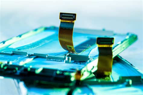
Flex PCB panelization has emerged as a pivotal innovation in the realm of electronics manufacturing, offering a multitude of advantages that cater to the evolving demands of modern technology. As electronic devices become increasingly compact and complex, the need for efficient and reliable circuit board solutions has never been more critical. Flex PCBs, or flexible printed circuit boards, have gained prominence due to their ability to bend and conform to various shapes, making them ideal for applications where space and flexibility are paramount. The process of panelization, which involves grouping multiple circuit boards onto a single panel for manufacturing, has undergone significant advancements, further enhancing the utility and efficiency of flex PCBs.
One of the primary innovations in flex PCB panelization technology is the development of advanced design software that allows for precise and efficient layout planning.
This software enables engineers to optimize the arrangement of circuits on a panel, minimizing waste and reducing production costs. By simulating various configurations, designers can identify the most effective panel layout, ensuring that the maximum number of boards can be produced from a single sheet of material. This not only conserves resources but also accelerates the manufacturing process, allowing for quicker turnaround times and increased production capacity.
Moreover, advancements in materials used for flex PCBs have significantly contributed to the evolution of panelization techniques.
The introduction of high-performance substrates and adhesives has enhanced the durability and reliability of flex PCBs, even in demanding environments. These materials offer improved thermal stability and resistance to environmental factors, ensuring that the circuits maintain their integrity over time. Consequently, manufacturers can produce flex PCBs that are not only more robust but also capable of supporting higher-density circuits, which is essential for modern electronic devices that require intricate and compact designs.
In addition to material innovations, the integration of automated manufacturing processes has revolutionized flex PCB panelization.
Automation technologies, such as robotic assembly and precision cutting, have streamlined the production process, reducing the likelihood of human error and ensuring consistent quality across all panels. These automated systems can handle complex panelization tasks with remarkable accuracy, allowing for the production of highly intricate designs that would be challenging to achieve manually. As a result, manufacturers can meet the stringent quality standards demanded by industries such as aerospace, automotive, and consumer electronics.
Furthermore, the implementation of advanced inspection and testing methods has bolstered the reliability of flex PCBs produced through panelization.
Techniques such as automated optical inspection (AOI) and X-ray inspection provide thorough quality checks, identifying defects or inconsistencies that may arise during production. By ensuring that each panel meets rigorous quality criteria, manufacturers can deliver products that are both reliable and efficient, minimizing the risk of failure in critical applications.
In conclusion, the innovations in flex PCB panelization technology have significantly enhanced the capabilities and applications of flexible circuit boards. Through advancements in design software, materials, automation, and inspection methods, manufacturers can produce high-quality flex PCBs that meet the demands of modern electronic devices. As technology continues to evolve, the importance of efficient and reliable circuit board solutions will only grow, making flex PCB panelization an indispensable component of the electronics manufacturing industry.