Flex pcb resistance
Understanding Flex PCB Resistance: Key Factors and Considerations
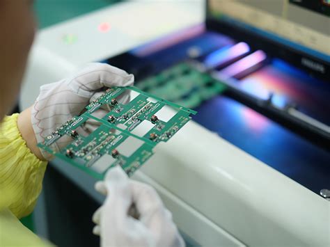
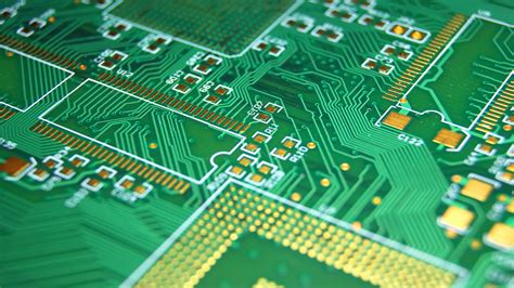
Flex PCBs, or flexible printed circuit boards, have become increasingly popular in various industries due to their versatility and ability to conform to complex shapes. Understanding the resistance characteristics of flex PCBs is crucial for optimizing their performance in electronic applications. Resistance in flex PCBs is influenced by several factors, including material properties, design considerations, and environmental conditions. By examining these elements, engineers and designers can make informed decisions to enhance the functionality and reliability of their flex PCB applications.
To begin with, the material composition of a flex PCB plays a significant role in determining its resistance.
Typically, flex PCBs are made from a combination of conductive materials, such as copper, and insulating substrates, like polyimide. The thickness and width of the copper traces directly affect the resistance; thinner and narrower traces exhibit higher resistance due to the reduced cross-sectional area available for current flow. Consequently, selecting the appropriate trace dimensions is essential to minimize resistance while maintaining the desired flexibility of the PCB.
In addition to material properties, the design of the flex PCB is another critical factor influencing resistance.
The layout of the circuit, including the length and routing of traces, can significantly impact resistance levels. Longer traces inherently possess higher resistance, as the electrons encounter more opposition as they travel through the conductor. Therefore, optimizing trace routing to minimize length and avoid unnecessary bends can help reduce resistance. Furthermore, incorporating ground planes and using multiple layers can enhance current distribution and decrease overall resistance.
Moreover, the choice of connectors and vias in a flex PCB design can also affect resistance.
Connectors serve as the interface between the flex PCB and other components, and their quality and design can introduce additional resistance. Ensuring that connectors are properly aligned and securely attached can mitigate this issue. Similarly, vias, which are used to connect different layers of a PCB, can contribute to resistance if not designed correctly. Utilizing plated-through holes and optimizing via placement can help minimize resistance and improve electrical performance.
Environmental conditions are another aspect that can influence the resistance of flex PCBs.
Temperature fluctuations, humidity, and exposure to harsh chemicals can alter the material properties of the PCB, leading to changes in resistance. For instance, increased temperatures can cause the copper traces to expand, potentially increasing resistance. Therefore, it is essential to consider the operating environment when designing and selecting materials for flex PCBs. Implementing protective coatings and selecting materials with stable thermal properties can help mitigate the effects of environmental factors on resistance.
In conclusion, understanding the resistance characteristics of flex PCBs is vital for ensuring their optimal performance in electronic applications. By considering material properties, design elements, and environmental conditions, engineers and designers can effectively manage resistance levels in flex PCBs. This comprehensive approach not only enhances the reliability and efficiency of the PCB but also extends its lifespan in various applications. As technology continues to advance, the demand for flexible and reliable electronic solutions will only grow, making the understanding of flex PCB resistance increasingly important for future innovations.

How Material Choices Impact Flex PCB Resistance
In the realm of modern electronics, flexible printed circuit boards (flex PCBs) have emerged as a pivotal component, offering versatility and adaptability in various applications. One of the critical aspects of flex PCBs is their electrical resistance, which can significantly influence the performance and reliability of electronic devices. Understanding how material choices impact flex PCB resistance is essential for engineers and designers aiming to optimize their designs for efficiency and durability.
To begin with, the substrate material of a flex PCB plays a crucial role in determining its resistance.
Polyimide is the most commonly used substrate due to its excellent thermal stability, mechanical strength, and flexibility. Its low dielectric constant and loss tangent contribute to reduced signal loss, thereby minimizing resistance. However, alternative materials such as polyester and liquid crystal polymer (LCP) are also employed, each offering distinct electrical properties. Polyester, for instance, is more cost-effective but may exhibit higher resistance due to its lower thermal stability and dielectric performance compared to polyimide. On the other hand, LCP provides superior electrical performance with lower resistance, making it suitable for high-frequency applications, albeit at a higher cost.
Transitioning to the conductive materials used in flex PCBs, copper is the predominant choice due to its excellent conductivity and availability.
The thickness of the copper layer is a significant factor affecting resistance; thicker copper layers generally result in lower resistance, enhancing the current-carrying capacity of the circuit. However, increasing the copper thickness can also lead to reduced flexibility, which may not be desirable in certain applications. Therefore, a balance must be struck between achieving low resistance and maintaining the necessary flexibility.
Moreover, the choice of adhesive materials used to bond the layers of a flex PCB can also impact resistance.
Adhesives with high dielectric constants can introduce additional resistance, affecting the overall performance of the circuit. Selecting adhesives with low dielectric constants and high thermal stability can help mitigate this issue, ensuring that the flex PCB maintains its electrical integrity under various operating conditions.
In addition to material selection, the design and layout of the flex PCB can influence its resistance.
The width and length of the conductive traces are critical parameters; wider and shorter traces typically exhibit lower resistance, facilitating better electrical performance. However, the need for compact designs often necessitates narrower traces, which can increase resistance. Employing advanced design techniques, such as using multiple layers or incorporating ground planes, can help manage resistance while accommodating space constraints.
Furthermore, environmental factors such as temperature and humidity can affect the resistance of flex PCBs.
High temperatures can cause the substrate and adhesive materials to expand, potentially increasing resistance. Similarly, exposure to moisture can lead to oxidation of the copper traces, further elevating resistance levels. Therefore, selecting materials with high thermal and moisture resistance is vital for ensuring the long-term reliability of flex PCBs.
In conclusion, the resistance of flex PCBs is intricately linked to the materials used in their construction. By carefully selecting substrate, conductive, and adhesive materials, and considering design and environmental factors, engineers can effectively manage resistance to optimize the performance of flex PCBs. As technology continues to advance, ongoing research and development in material science will undoubtedly lead to further innovations, enhancing the capabilities and applications of flex PCBs in the ever-evolving landscape of electronics.
Techniques to Minimize Resistance in Flex PCBs
Flex PCBs, or flexible printed circuit boards, have become increasingly popular in various industries due to their ability to bend and conform to different shapes, making them ideal for compact and complex electronic devices. However, one of the challenges associated with flex PCBs is managing their electrical resistance, which can impact the performance and efficiency of the electronic device. Therefore, understanding and implementing techniques to minimize resistance in flex PCBs is crucial for engineers and designers.
To begin with, selecting the appropriate materials is fundamental in reducing resistance in flex PCBs.
Conductive materials such as copper are commonly used due to their excellent electrical conductivity. However, the thickness of the copper layer plays a significant role in determining the resistance. Thicker copper layers generally offer lower resistance, but they also increase the weight and cost of the PCB. Therefore, a balance must be struck between minimizing resistance and maintaining the desired flexibility and cost-effectiveness of the PCB.
In addition to material selection, the design of the circuit layout is another critical factor in minimizing resistance.
Shorter and wider traces are preferred as they reduce the path length for current flow, thereby decreasing resistance. Moreover, using multiple layers for routing can help distribute the current more evenly, further reducing resistance. It is also beneficial to avoid sharp bends and corners in the trace design, as these can create points of high resistance and potential failure.
Furthermore, the use of advanced manufacturing techniques can significantly impact the resistance of flex PCBs.
For instance, employing high-precision etching processes ensures that the traces are uniform and free from defects, which can otherwise increase resistance. Additionally, techniques such as laser drilling can be used to create vias with minimal resistance, enhancing the overall conductivity of the PCB.
Another effective approach to minimizing resistance is through the implementation of surface treatments and coatings.
These treatments can protect the conductive traces from oxidation and corrosion, which can increase resistance over time. For example, applying a layer of gold or silver plating can enhance conductivity and provide a protective barrier against environmental factors. Moreover, using solder masks can prevent short circuits and maintain the integrity of the conductive paths.
Thermal management is also a crucial consideration in reducing resistance in flex PCBs.
Excessive heat can increase the resistance of conductive materials, leading to performance degradation. Therefore, incorporating thermal vias and heat sinks can help dissipate heat effectively, maintaining optimal operating conditions for the PCB. Additionally, selecting materials with high thermal conductivity can aid in efficient heat distribution, further minimizing resistance.
Finally, regular testing and quality control are essential to ensure that the flex PCBs meet the desired resistance specifications.
Employing techniques such as impedance spectroscopy and time-domain reflectometry can help identify areas of high resistance and potential defects. By addressing these issues early in the design and manufacturing process, engineers can ensure that the final product performs reliably and efficiently.
In conclusion, minimizing resistance in flex PCBs requires a comprehensive approach that encompasses material selection, circuit design, manufacturing techniques, surface treatments, thermal management, and rigorous testing. By carefully considering each of these factors, engineers can optimize the performance of flex PCBs, ensuring their suitability for a wide range of applications in modern electronic devices.

The Role of Design in Managing Flex PCB Resistance
In the realm of modern electronics, flexible printed circuit boards (PCBs) have emerged as a pivotal component, offering versatility and adaptability in various applications.
One of the critical aspects of flex PCBs is their electrical resistance, which can significantly impact the performance and reliability of electronic devices.
Understanding the role of design in managing flex PCB resistance is essential for engineers and designers striving to optimize their products.
To begin with, the resistance of a flex PCB is influenced by several factors, including the materials used, the thickness of the conductive layers, and the overall geometry of the circuit. The choice of materials is paramount, as it directly affects the conductivity and, consequently, the resistance of the circuit.
Copper is the most commonly used material for conductive traces due to its excellent electrical properties. However, the thickness of the copper layer must be carefully considered. Thicker copper layers reduce resistance but may increase the board’s weight and cost, while thinner layers may lead to higher resistance and potential performance issues.
Moreover, the design of the circuit layout plays a crucial role in managing resistance.
The length and width of the conductive traces are significant factors; longer traces inherently possess higher resistance due to the increased path for electron flow. Therefore, minimizing trace length through efficient layout design is a fundamental strategy in reducing resistance. Additionally, increasing the width of the traces can lower resistance, as a wider path allows more electrons to flow simultaneously. However, this must be balanced with the available space on the PCB and the specific design requirements of the application.
Transitioning to another critical aspect, the bending and flexing of the PCB can also affect its resistance.
Flex PCBs are designed to withstand mechanical stress, but repeated bending can lead to micro-cracks in the conductive traces, increasing resistance over time. To mitigate this, designers can incorporate features such as curved traces and stress-relief patterns, which distribute mechanical stress more evenly across the board. These design elements help maintain the integrity of the conductive paths, ensuring consistent resistance levels even under dynamic conditions.
Furthermore, the environment in which the flex PCB operates can influence its resistance.
Factors such as temperature, humidity, and exposure to chemicals can alter the material properties of the PCB, affecting its resistance. Designing for environmental resilience involves selecting materials and protective coatings that can withstand these conditions without significant degradation. For instance, using polyimide substrates, known for their thermal stability and chemical resistance, can help maintain consistent resistance levels in harsh environments.
In addition to these considerations, advanced simulation tools and software can aid designers in predicting and managing resistance in flex PCBs.
By modeling the electrical and mechanical behavior of the circuit, designers can identify potential issues and optimize the layout before physical prototyping. This proactive approach not only saves time and resources but also enhances the reliability and performance of the final product.
In conclusion, the design of flex PCBs plays a vital role in managing their resistance, impacting the overall functionality and durability of electronic devices. By carefully selecting materials, optimizing circuit layouts, and considering environmental factors, designers can effectively control resistance levels. As technology continues to evolve, the importance of thoughtful design in managing flex PCB resistance will remain a cornerstone of successful electronic product development.