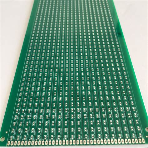
Flex pcb stack up
Understanding The Basics Of Flex PCB Stack Up
In the realm of modern electronics, the design and implementation of flexible printed circuit boards (PCBs) have become increasingly significant. As devices continue to shrink in size while expanding in functionality, the demand for innovative solutions like flex PCBs has surged. Understanding the basics of flex PCB stack up is crucial for engineers and designers aiming to optimize the performance and reliability of their electronic products.
Flex PCBs, unlike their rigid counterparts, offer the advantage of bending and folding, which allows for more compact and versatile designs.
This flexibility is achieved through a unique stack-up configuration that involves multiple layers of conductive and insulating materials. The stack-up of a flex PCB is a critical aspect that determines its electrical performance, mechanical durability, and overall functionality. Therefore, a comprehensive understanding of the stack-up process is essential for anyone involved in the design and manufacturing of these advanced circuits.
To begin with, the stack-up of a flex PCB typically consists of several layers, each serving a distinct purpose.
The core layer, often made of a flexible substrate such as polyimide, provides the foundational support for the circuit. This material is chosen for its excellent thermal stability and mechanical flexibility, which are essential for maintaining the integrity of the circuit under various conditions. On top of the core layer, conductive layers made of copper are added. These layers form the electrical pathways that connect different components of the circuit. The number of conductive layers can vary depending on the complexity of the design, with more layers allowing for more intricate circuitry.
In addition to the core and conductive layers, flex PCBs also include insulating layers.
These layers, typically made of materials like adhesive or coverlay, serve to protect the conductive traces from environmental factors such as moisture and dust. They also provide electrical insulation between different conductive layers, preventing short circuits and ensuring the reliability of the circuit. The choice of insulating materials and their thickness can significantly impact the flexibility and durability of the final product.
Moreover, the stack-up process involves careful consideration of the alignment and bonding of these layers.
Precise alignment is crucial to ensure that the conductive traces are accurately positioned, which is vital for the circuit’s functionality. Bonding, on the other hand, involves the use of heat and pressure to adhere the layers together, forming a cohesive and durable structure. The quality of bonding directly affects the mechanical strength and flexibility of the flex PCB, making it a critical step in the manufacturing process.
Transitioning from the technical aspects, it is important to note that the design of a flex PCB stack-up is not a one-size-fits-all solution.
Each application may require a unique configuration to meet specific performance and environmental requirements. Factors such as the operating temperature, mechanical stress, and electrical load must be considered when designing the stack-up. Additionally, advancements in materials and manufacturing techniques continue to expand the possibilities for flex PCB designs, offering new opportunities for innovation in electronic devices.
In conclusion, understanding the basics of flex PCB stack-up is essential for optimizing the performance and reliability of flexible circuits. By carefully selecting and configuring the various layers, designers can create circuits that meet the demanding requirements of modern electronic applications. As technology continues to evolve, the role of flex PCBs in enabling smaller, more efficient, and more versatile devices will undoubtedly grow, making knowledge of their stack-up an invaluable asset in the field of electronics design.
Key Considerations For Designing Flex PCB Stack Up
When designing a flex PCB stack-up, several key considerations must be taken into account to ensure optimal performance and reliability. Flex PCBs, or flexible printed circuit boards, offer unique advantages over traditional rigid PCBs, such as the ability to bend and conform to complex shapes. This flexibility makes them ideal for applications in compact and dynamic environments, such as wearable technology, medical devices, and aerospace systems. However, the design of a flex PCB stack-up requires careful attention to detail to address the specific challenges associated with their use.
To begin with, material selection is a critical factor in the design of a flex PCB stack-up.
The choice of materials affects not only the flexibility and durability of the PCB but also its electrical performance. Polyimide is a commonly used substrate material due to its excellent thermal stability and mechanical properties. It is essential to consider the dielectric constant and loss tangent of the materials, as these will influence signal integrity, especially in high-frequency applications. Additionally, the adhesive used in the stack-up must be chosen carefully to ensure it can withstand the mechanical stresses and environmental conditions the PCB will encounter.
Another important consideration is the layer configuration within the stack-up.
The number of layers and their arrangement can significantly impact the flexibility and functionality of the PCB. A single-layer flex PCB offers maximum flexibility but may not provide sufficient routing options for complex designs. Conversely, a multi-layer stack-up can accommodate more intricate circuits but may reduce flexibility. Designers must strike a balance between these factors, taking into account the specific requirements of the application. Furthermore, the use of cross-hatched ground planes instead of solid ones can enhance flexibility while maintaining electrical performance.
The thickness of the flex PCB is another crucial aspect to consider.
Thinner PCBs are generally more flexible, but they may also be more prone to mechanical damage. Therefore, it is vital to determine the appropriate thickness that provides the necessary flexibility without compromising the structural integrity of the PCB. This decision should be informed by the bend radius requirements of the application, as exceeding the minimum bend radius can lead to mechanical failure.
In addition to these considerations, the design of the flex PCB stack-up must also account for thermal management.
Flex PCBs can be subject to significant temperature variations, which can affect their performance and longevity. Effective thermal management strategies, such as the use of thermal vias and heat spreaders, can help dissipate heat and maintain the reliability of the PCB. Moreover, the choice of materials with good thermal conductivity can further enhance the thermal performance of the stack-up.
Finally, manufacturability is a key consideration in the design of a flex PCB stack-up.
The design must be compatible with existing manufacturing processes to ensure cost-effectiveness and scalability. This includes considering factors such as the minimum trace width and spacing, as well as the tolerances for drilling and etching. Collaborating with experienced manufacturers during the design phase can help identify potential challenges and optimize the design for production.
In conclusion, designing a flex PCB stack-up involves a complex interplay of material selection, layer configuration, thickness determination, thermal management, and manufacturability. By carefully considering these factors, designers can create flex PCBs that meet the specific demands of their applications, ensuring both performance and reliability.
Common Challenges In Flex PCB Stack Up And How To Overcome Them
In the realm of modern electronics, the demand for compact, lightweight, and flexible devices has led to the increased adoption of flexible printed circuit boards (PCBs). These innovative circuits offer numerous advantages, including the ability to bend and fold, which is particularly beneficial in applications where space is limited. However, designing and manufacturing flex PCBs come with their own set of challenges, particularly in the stack-up process. Understanding these challenges and how to overcome them is crucial for engineers and designers aiming to optimize the performance and reliability of their flex PCB designs.
One of the primary challenges in flex PCB stack-up is managing the mechanical stress that occurs during bending and flexing.
Unlike rigid PCBs, flex circuits are subjected to dynamic mechanical forces, which can lead to material fatigue and eventual failure. To mitigate this issue, it is essential to carefully select materials that can withstand repeated bending. Polyimide is a popular choice due to its excellent flexibility and thermal stability. Additionally, incorporating strain relief features, such as curved traces and staggered vias, can help distribute stress more evenly across the board, reducing the likelihood of mechanical failure.
Another significant challenge is ensuring signal integrity in the flex PCB stack-up.
As devices become more complex, maintaining high-speed signal transmission without interference is critical. The flexible nature of these circuits can introduce variations in impedance, which can degrade signal quality. To address this, designers must pay close attention to the dielectric materials used in the stack-up, as well as the thickness and spacing of the conductive layers. Implementing controlled impedance techniques and using low-loss materials can help maintain signal integrity, even in the most demanding applications.
Thermal management is also a crucial consideration in flex PCB stack-up.
The compact nature of these circuits often results in higher power densities, which can lead to overheating if not properly managed. Effective thermal management strategies include the use of thermal vias, heat sinks, and thermal interface materials to dissipate heat away from critical components. Additionally, selecting materials with high thermal conductivity can enhance heat dissipation, ensuring the longevity and reliability of the flex PCB.
Furthermore, the manufacturing process itself presents challenges in flex PCB stack-up.
The flexible nature of these circuits can complicate the lamination process, leading to issues such as misalignment and delamination. To overcome these challenges, it is essential to work closely with experienced manufacturers who understand the nuances of flex PCB production. Employing advanced manufacturing techniques, such as laser drilling and precision alignment tools, can help ensure accurate layer registration and robust lamination.
Finally, cost considerations cannot be overlooked when addressing challenges in flex PCB stack-up.
The specialized materials and processes required for these circuits can lead to higher production costs compared to traditional rigid PCBs. To manage costs effectively, designers should focus on optimizing the stack-up design to minimize material usage and simplify the manufacturing process. Collaborating with suppliers to source cost-effective materials and exploring alternative design approaches can also contribute to cost savings.
In conclusion, while flex PCB stack-up presents several challenges, understanding and addressing these issues is essential for successful design and manufacturing. By carefully selecting materials, implementing effective design strategies, and collaborating with experienced manufacturers, engineers can overcome these challenges and harness the full potential of flex PCBs in their applications. As technology continues to evolve, the ability to navigate these complexities will be crucial in meeting the growing demand for flexible, high-performance electronic devices.
Innovations And Trends In Flex PCB Stack Up Technology
Flex PCB stack-up technology has witnessed significant advancements in recent years, driven by the increasing demand for more compact, efficient, and versatile electronic devices. As the electronics industry continues to evolve, the need for flexible printed circuit boards (PCBs) that can accommodate complex designs and functionalities has become paramount. This has led to innovations in flex PCB stack-up technology, which are reshaping the landscape of electronic manufacturing.
One of the most notable trends in flex PCB stack-up technology is the development of multi-layer flex PCBs.
Traditionally, flex PCBs were limited to single or double layers, which restricted their application in more sophisticated electronic devices. However, with the advent of multi-layer flex PCBs, designers can now incorporate more complex circuitry within a smaller footprint. This innovation not only enhances the functionality of electronic devices but also allows for greater design flexibility, enabling the creation of more intricate and compact products.
In addition to multi-layer designs, the use of advanced materials in flex PCB stack-ups has also gained traction.
Materials such as polyimide and liquid crystal polymer (LCP) are increasingly being used due to their superior thermal stability, flexibility, and electrical performance. These materials allow for the production of flex PCBs that can withstand harsh environmental conditions, making them ideal for applications in industries such as aerospace, automotive, and medical devices. The integration of these advanced materials into flex PCB stack-ups is a testament to the ongoing efforts to enhance the durability and reliability of electronic components.
Moreover, the miniaturization of electronic components has necessitated the development of thinner and lighter flex PCBs.
This trend is particularly evident in the consumer electronics sector, where there is a constant push for slimmer and more portable devices. By reducing the thickness of the flex PCB stack-up, manufacturers can achieve a significant reduction in the overall weight and size of the device, without compromising on performance. This has opened up new possibilities for the design and functionality of electronic products, allowing for more innovative and user-friendly solutions.
Furthermore, the rise of the Internet of Things (IoT) has spurred the demand for flex PCBs with enhanced connectivity features.
As more devices become interconnected, the need for PCBs that can support wireless communication and data transfer has become critical. Innovations in flex PCB stack-up technology have led to the integration of antennas and other communication components directly into the PCB, streamlining the design and improving the efficiency of IoT devices. This development is crucial for the seamless operation of smart devices, which rely on reliable and efficient communication networks.
In conclusion, the innovations and trends in flex PCB stack-up technology are paving the way for a new era of electronic manufacturing. The advancements in multi-layer designs, the use of advanced materials, the push for miniaturization, and the integration of connectivity features are all contributing to the creation of more sophisticated and efficient electronic devices. As the demand for flexible and versatile PCBs continues to grow, it is clear that flex PCB stack-up technology will play a pivotal role in shaping the future of the electronics industry. These developments not only address current challenges but also set the stage for future innovations, ensuring that flex PCBs remain at the forefront of technological progress.