Flex pcb structure
Understanding The Layers Of Flex PCB Structure
Flexible printed circuit boards (Flex PCBs) have become an integral component in modern electronic devices, offering a unique combination of flexibility, durability, and space efficiency. To fully appreciate the advantages and applications of Flex PCBs, it is essential to understand their layered structure, which is meticulously designed to meet the demands of various electronic applications.
At the core of a Flex PCB is the substrate, typically made from a flexible polymer such as polyimide.
This material is chosen for its excellent thermal stability, mechanical strength, and flexibility, which are crucial for the dynamic environments in which Flex PCBs often operate. The substrate serves as the foundational layer upon which other layers are built, providing the necessary support and insulation for the conductive pathways.
Adhered to the substrate is the copper foil, which forms the conductive traces of the circuit.
The copper layer is usually deposited through a process called electroplating, ensuring a uniform and reliable conductive path. The thickness of the copper layer can vary depending on the specific requirements of the application, with thicker layers providing lower resistance and higher current-carrying capacity. The copper traces are meticulously patterned using photolithography, a process that involves coating the copper with a light-sensitive material, exposing it to a patterned light source, and then etching away the unexposed areas to create the desired circuit layout.
To protect the copper traces and ensure electrical insulation, a dielectric layer is applied over the copper.
This layer, often made from the same polyimide material as the substrate, serves to isolate the conductive pathways from each other and from external environmental factors. The dielectric layer is crucial for maintaining the integrity and performance of the Flex PCB, as it prevents short circuits and other electrical failures.
In addition to the dielectric layer, a coverlay or solder mask is often applied to further protect the circuit.
The coverlay is a flexible film that is laminated over the entire surface of the Flex PCB, providing additional mechanical protection and environmental resistance. The solder mask, on the other hand, is a liquid coating that is applied selectively to areas where soldering will occur, preventing solder bridges and ensuring precise connections.
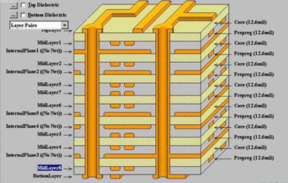
For multi-layer Flex PCBs, additional layers of copper and dielectric material are added in a sequential manner, with each layer being carefully aligned and bonded to the previous ones.
This multi-layer construction allows for more complex and compact circuit designs, enabling the integration of more functionality within a smaller footprint. The layers are interconnected through vias, which are small holes drilled through the layers and filled with conductive material to establish electrical connections between different layers.
Finally, the entire Flex PCB is often encapsulated in a protective coating or laminate to enhance its durability and resistance to environmental factors such as moisture, chemicals, and mechanical stress. This final layer ensures that the Flex PCB can withstand the rigors of its intended application, whether it be in consumer electronics, medical devices, automotive systems, or aerospace technology.
In conclusion, the layered structure of Flex PCBs is a testament to the intricate engineering and precise manufacturing processes that go into their production. Each layer plays a critical role in ensuring the performance, reliability, and flexibility of the final product, making Flex PCBs an indispensable component in the ever-evolving landscape of electronic technology.
Material Selection For Flex PCB Design
When designing flexible printed circuit boards (flex PCBs), the selection of materials is a critical factor that significantly influences the performance, reliability, and cost of the final product. Flex PCBs are known for their ability to bend and twist, making them ideal for applications where space constraints and mechanical flexibility are paramount. To achieve these characteristics, designers must carefully choose materials that not only meet the electrical and mechanical requirements but also withstand the environmental conditions to which the flex PCB will be exposed.
The base material of a flex PCB typically consists of a flexible substrate, which serves as the foundation for the circuit.
Polyimide is the most commonly used substrate material due to its excellent thermal stability, mechanical strength, and flexibility. Polyimide can withstand high temperatures, making it suitable for applications that involve soldering processes or operate in harsh environments. Additionally, its low dielectric constant and high dielectric strength ensure reliable electrical performance. However, polyimide is relatively expensive compared to other materials, which can impact the overall cost of the flex PCB.
In some cases, polyester (PET) is used as an alternative substrate mate
While PET is less expensive than polyimide, it has lower thermal stability and mechanical strength. Consequently, PET-based flex PCBs are typically used in applications with less demanding environmental and mechanical requirements. Despite these limitations, PET offers adequate electrical properties and can be a cost-effective solution for certain applications.
The conductive material used in flex PCBs is another crucial consideration.
Copper is the preferred choice due to its excellent electrical conductivity and ductility. Copper can be deposited onto the substrate using various methods, such as electroplating or laminating copper foil. The thickness of the copper layer can vary depending on the current-carrying requirements of the circuit. Thicker copper layers provide lower resistance and better current-carrying capacity but can reduce the flexibility of the PCB. Therefore, designers must strike a balance between electrical performance and mechanical flexibility.
To protect the copper traces and ensure the durability of the flex PCB, a coverlay or overlay material is applied.
Polyimide coverlay is commonly used due to its compatibility with the polyimide substrate and its ability to provide excellent mechanical protection and insulation. The coverlay material must be flexible enough to accommodate the bending and twisting of the flex PCB while maintaining its protective properties. In some designs, a flexible solder mask may be used as an alternative to coverlay, offering similar protective benefits with potentially lower costs.
Adhesives play a vital role in bonding the various layers of a flex PCB.
The choice of adhesive depends on factors such as the operating temperature, mechanical stress, and chemical exposure. Acrylic and epoxy adhesives are commonly used due to their strong bonding properties and thermal stability. However, the adhesive must be carefully selected to ensure it does not compromise the flexibility of the PCB.
In conclusion, the selection of materials for flex PCB design is a complex process that requires careful consideration of various factors, including electrical performance, mechanical flexibility, thermal stability, and cost. By understanding the properties and trade-offs of different materials, designers can create flex PCBs that meet the specific requirements of their applications while ensuring reliability and durability. The interplay between substrate, conductive materials, protective layers, and adhesives ultimately determines the success of the flex PCB in its intended application.
Advantages Of Using Flex PCBs In Modern Electronics
Flex PCBs, or flexible printed circuit boards, have become increasingly prevalent in modern electronics due to their numerous advantages over traditional rigid PCBs. One of the primary benefits of using flex PCBs is their ability to conform to various shapes and sizes, which allows for greater design flexibility. This adaptability is particularly valuable in applications where space constraints are a significant concern, such as in wearable technology, medical devices, and compact consumer electronics. By enabling more efficient use of available space, flex PCBs contribute to the miniaturization of electronic devices, a trend that continues to dominate the industry.
In addition to their physical flexibility, flex PCBs offer enhanced durability and reliability.
The materials used in their construction, such as polyimide or polyester films, provide excellent resistance to environmental factors like heat, moisture, and chemicals. This resilience ensures that flex PCBs can withstand harsh operating conditions, making them suitable for use in automotive, aerospace, and industrial applications. Furthermore, the inherent flexibility of these circuits reduces the risk of mechanical failure due to vibrations or bending, thereby extending the lifespan of the electronic devices in which they are used.
Another significant advantage of flex PCBs is their potential for reducing the overall weight and thickness of electronic assemblies.
Traditional rigid PCBs often require additional connectors and cables to achieve the same level of functionality, which can add bulk and complexity to the design. In contrast, flex PCBs can integrate multiple layers and components into a single, streamlined structure, eliminating the need for extra interconnections. This reduction in weight and thickness is particularly beneficial in portable and handheld devices, where every gram and millimeter count.
Moreover, flex PCBs can lead to cost savings in both manufacturing and assembly processes.
The ability to fold and bend these circuits allows for more efficient use of materials, reducing waste and lowering production costs. Additionally, the simplified assembly process associated with flex PCBs can result in shorter production times and fewer assembly errors. This efficiency translates to lower labor costs and improved yield rates, making flex PCBs an economically attractive option for many manufacturers.
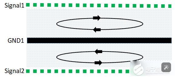
The versatility of flex PCBs also extends to their electrical performance.
The design flexibility allows for optimized routing of signal paths, which can minimize electromagnetic interference (EMI) and crosstalk between components. This improved signal integrity is crucial in high-speed and high-frequency applications, where maintaining the quality of electrical signals is paramount. Furthermore, the ability to incorporate components directly onto the flex PCB substrate can enhance the overall performance of the electronic system by reducing parasitic inductance and capacitance.
In conclusion, the advantages of using flex PCBs in modern electronics are manifold. Their ability to conform to various shapes and sizes, coupled with their enhanced durability and reliability, makes them an ideal choice for a wide range of applications. The potential for reducing weight and thickness, along with cost savings in manufacturing and assembly, further underscores their value. Additionally, the improved electrical performance offered by flex PCBs ensures that they will continue to play a critical role in the advancement of electronic technology. As the demand for smaller, more efficient, and more reliable electronic devices grows, the adoption of flex PCBs is likely to increase, solidifying their position as a cornerstone of modern electronics design.
Common Challenges In Flex PCB Manufacturing And Solutions
Flex PCBs, or flexible printed circuit boards, have become increasingly popular in various industries due to their versatility, lightweight nature, and ability to conform to complex shapes. However, the manufacturing of flex PCBs presents several challenges that can impact their performance and reliability. Understanding these challenges and implementing effective solutions is crucial for producing high-quality flex PCBs.
One of the primary challenges in flex PCB manufacturing is material selection. Flex PCBs are typically made from polyimide or polyester films, which offer excellent flexibility and thermal stability. However, these materials can be more expensive and difficult to handle compared to traditional rigid PCB materials. To address this, manufacturers must carefully balance cost and performance by selecting materials that meet the specific requirements of the application while also considering factors such as thickness, flexibility, and thermal properties.
Another significant challenge is the design complexity associated with flex PCBs.
Unlike rigid PCBs, flex PCBs must be designed to accommodate bending, folding, and twisting without compromising electrical performance. This requires careful consideration of trace routing, pad placement, and layer stack-up to ensure that the PCB can withstand mechanical stress without causing signal integrity issues or mechanical failure. Advanced design software and simulation tools can help engineers optimize the layout and predict potential issues before fabrication, thereby reducing the risk of costly design iterations.
Manufacturing process control is also a critical aspect of flex PCB production.
The thin and flexible nature of the substrate makes it susceptible to handling damage, misalignment, and warping during the manufacturing process. To mitigate these risks, manufacturers must implement stringent process controls and quality assurance measures. This includes using specialized equipment for material handling, precise alignment tools for layer registration, and automated inspection systems to detect defects early in the production process.
Thermal management is another challenge that must be addressed in flex PCB manufacturing.
The flexible materials used in these PCBs typically have lower thermal conductivity compared to rigid materials, which can lead to heat buildup and potential failure in high-power applications. To overcome this, manufacturers can incorporate thermal vias, heat sinks, and other thermal management techniques into the design. Additionally, selecting materials with higher thermal conductivity and optimizing the PCB layout to minimize heat generation can further enhance thermal performance.
Adhesion between the various layers of a flex PCB is also a critical factor that can impact reliability.
Poor adhesion can lead to delamination, which can cause electrical failures and reduce the overall lifespan of the PCB. To ensure strong adhesion, manufacturers must carefully control the lamination process, including temperature, pressure, and time. Using high-quality adhesives and surface treatments can also improve bonding strength and reduce the risk of delamination.
Finally, testing and validation are essential steps in the flex PCB manufacturing process.
Due to the unique mechanical properties of flex PCBs, traditional testing methods may not be sufficient to identify potential issues. Manufacturers must develop specialized testing protocols that simulate the real-world conditions the PCB will encounter, including bending, twisting, and thermal cycling. This ensures that the final product meets the required performance and reliability standards.
In conclusion, while flex PCB manufacturing presents several challenges, these can be effectively managed through careful material selection, advanced design techniques, stringent process controls, and thorough testing. By addressing these challenges, manufacturers can produce high-quality flex PCBs that meet the demanding requirements of modern electronic applications.