Flex pcb types
Single-Sided Flex pcb types: Applications And Benefits
Single-sided flexible printed circuit boards (PCBs) are a fundamental component in the realm of modern electronics, offering a unique combination of flexibility, durability, and cost-effectiveness.
These PCBs consist of a single conductive layer of metal, typically copper, which is laminated onto a flexible dielectric substrate. The simplicity of their design makes them an attractive option for a variety of applications, particularly where space constraints and mechanical flexibility are paramount.
One of the primary applications of single-sided flex PCBs is in consumer electronics.
Devices such as smartphones, tablets, and wearable technology often require compact and lightweight components that can withstand repeated bending and flexing. Single-sided flex PCBs meet these requirements by providing a thin, flexible solution that can be easily integrated into the tight confines of modern electronic devices. Additionally, their ability to conform to various shapes and contours allows for innovative product designs that would be impossible with rigid PCBs.
In the automotive industry, single-sided flex PCBs are utilized in a range of applications, from dashboard displays to advanced driver-assistance systems (ADAS).
The harsh operating conditions within vehicles, including exposure to extreme temperatures and vibrations, necessitate components that are both robust and reliable. Single-sided flex PCBs excel in these environments due to their inherent flexibility and resilience. Moreover, their lightweight nature contributes to the overall reduction in vehicle weight, which is a critical factor in improving fuel efficiency and reducing emissions.
Medical devices also benefit significantly from the use of single-sided flex PCBs.
In applications such as diagnostic equipment, wearable health monitors, and implantable devices, the need for miniaturization and flexibility is paramount. Single-sided flex PCBs enable the development of compact, lightweight medical devices that can be comfortably worn or implanted in the human body. Their biocompatibility and ability to endure sterilization processes further enhance their suitability for medical applications.
The aerospace and defense sectors similarly leverage the advantages of single-sided flex PCBs.
In these industries, the demand for reliable, high-performance components that can operate under extreme conditions is critical. Single-sided flex PCBs are employed in various applications, including satellite systems, avionics, and military communication devices. Their ability to maintain functionality in the face of intense vibrations, temperature fluctuations, and radiation exposure makes them an indispensable component in aerospace and defense technologies.
Beyond their diverse applications, single-sided flex PCBs offer several benefits that contribute to their widespread adoption.
One notable advantage is their cost-effectiveness. The manufacturing process for single-sided flex PCBs is relatively straightforward, involving fewer layers and materials compared to multi-layered alternatives. This simplicity translates to lower production costs, making them an economical choice for many applications.
Furthermore, single-sided flex PCBs provide excellent electrical performance. The absence of multiple layers reduces the potential for signal interference and crosstalk, ensuring reliable and efficient signal transmission. This characteristic is particularly important in high-frequency applications where signal integrity is crucial.
In conclusion, single-sided flex PCBs are a versatile and valuable component in various industries, offering a unique blend of flexibility, durability, and cost-effectiveness. Their applications span consumer electronics, automotive, medical, aerospace, and defense sectors, where their ability to conform to complex shapes and endure harsh conditions is highly prized. The benefits of single-sided flex PCBs, including their cost-effectiveness and superior electrical performance, further underscore their importance in the ever-evolving landscape of modern electronics.

Double-Sided Flex PCBs: Design And Manufacturing Insights
Double-sided flexible printed circuit boards (PCBs) represent a significant advancement in the realm of electronic design and manufacturing. These PCBs, characterized by their ability to accommodate conductive pathways on both sides of a flexible substrate, offer a unique combination of flexibility and functionality.
This dual-sided configuration allows for more complex circuitry within a compact form factor, making them ideal for a variety of applications, from consumer electronics to medical devices.
The design of double-sided flex PCBs begins with the selection of appropriate materials. Typically, a polyimide film is used as the substrate due to its excellent thermal stability, mechanical strength, and flexibility. This substrate is then laminated with a thin layer of copper on both sides, which serves as the conductive material. The choice of copper thickness is crucial, as it must balance the need for electrical conductivity with the requirement for flexibility. Thinner copper layers enhance flexibility but may limit current-carrying capacity, whereas thicker layers improve conductivity but reduce the board’s ability to bend.
Once the materials are selected, the design process involves creating a detailed layout of the circuitry.
Advanced computer-aided design (CAD) software is employed to map out the intricate network of traces, pads, and vias that will form the electrical connections. In double-sided flex PCBs, vias play a critical role as they enable electrical connections between the two layers. These vias can be either through-hole, which pass completely through the substrate, or blind/buried, which connect only specific layers. The choice of via type depends on the complexity and requirements of the circuit.
Transitioning from design to manufacturing, the process begins with the application of a photoresist to the copper-clad substrate.
photoresist is then exposed to ultraviolet light through a mask that defines the desired circuit pattern. The exposed areas of the photoresist harden, while the unexposed areas remain soft and are subsequently washed away. This leaves a precise pattern of photoresist on the copper, which acts as a protective barrier during the etching process. The substrate is then subjected to a chemical etchant that removes the unprotected copper, leaving behind the desired circuit traces.
Following the etching process, the next step involves drilling the vias.
Precision drilling equipment is used to create the necessary holes, which are then plated with copper to establish electrical connections between the layers. This plating process is critical, as it ensures the reliability and conductivity of the vias. After plating, additional layers of protective materials, such as solder mask and coverlay, are applied to shield the circuitry from environmental factors and mechanical damage.
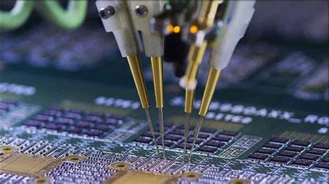
Quality control is an integral part of the manufacturing process.
Each double-sided flex PCB undergoes rigorous testing to ensure it meets the specified electrical and mechanical requirements. Automated optical inspection (AOI) systems are used to detect any defects in the circuitry, while electrical testing verifies the continuity and integrity of the connections. Any deviations from the design specifications are addressed before the final product is approved for use.
In conclusion, double-sided flex PCBs offer a versatile solution for modern electronic applications, combining the benefits of flexible substrates with the complexity of dual-layer circuitry. The design and manufacturing processes are intricate and require careful consideration of materials, layout, and quality control to ensure optimal performance. As technology continues to advance, the demand for these innovative PCBs is likely to grow, driving further developments in their design and production techniques.
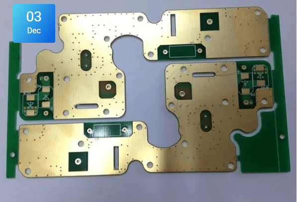
Multilayer Flex PCBs: Advanced Solutions For Complex Designs
Multilayer Flex PCBs: Advanced Solutions For Complex Designs
In the realm of modern electronics, the demand for compact, efficient, and reliable devices has led to significant advancements in printed circuit board (PCB) technology. Among these innovations, multilayer flexible PCBs have emerged as a pivotal solution for complex electronic designs. These advanced PCBs offer a unique combination of flexibility, durability, and high performance, making them indispensable in various high-tech applications.
Multilayer flex PCBs consist of multiple layers of conductive material, typically copper, separated by insulating layers of polyimide or other flexible substrates.
This construction allows for intricate circuit designs that can be folded, twisted, or bent without compromising the integrity of the electrical connections. Consequently, multilayer flex PCBs are particularly well-suited for applications where space constraints and mechanical stress are significant considerations.
One of the primary advantages of multilayer flex PCBs is their ability to support high-density interconnections.
By stacking multiple layers of circuitry, designers can achieve a greater number of connections within a smaller footprint compared to traditional single-layer or double-layer PCBs. This capability is crucial in the development of miniaturized electronic devices, such as smartphones, wearable technology, and medical implants, where every millimeter of space is valuable.
Moreover, the flexibility of these PCBs enhances their reliability in dynamic environments.
Unlike rigid PCBs, which can crack or break under mechanical stress, multilayer flex PCBs can withstand repeated bending and flexing. This resilience is particularly beneficial in applications such as aerospace, automotive, and industrial machinery, where electronic components are often subjected to vibrations, shocks, and other mechanical forces.
In addition to their mechanical advantages, multilayer flex PCBs also offer superior electrical performance.
The use of multiple layers allows for the separation of power and signal traces, reducing electromagnetic interference (EMI) and crosstalk. This separation is essential in high-speed and high-frequency applications, where signal integrity is paramount. Furthermore, the ability to incorporate ground planes and shielding layers within the PCB stack-up enhances the overall electromagnetic compatibility (EMC) of the design.
The manufacturing process of multilayer flex PCBs is more complex than that of their single-layer counterparts.
It involves precise alignment and lamination of multiple layers, as well as advanced techniques such as via formation and laser drilling. Despite these challenges, advancements in fabrication technology have made it possible to produce multilayer flex PCBs with high precision and consistency. As a result, these PCBs can meet the stringent quality and performance standards required in critical applications.
Another noteworthy aspect of multilayer flex PCBs is their potential for integration with rigid PCBs, resulting in rigid-flex PCBs. This hybrid approach combines the best of both worlds: the flexibility of flex PCBs and the robustness of rigid PCBs. Rigid-flex PCBs are particularly advantageous in applications where a combination of rigid and flexible sections is needed, such as in complex electronic assemblies with multiple interconnected modules.
In conclusion, multilayer flex PCBs represent a sophisticated solution for addressing the challenges of modern electronic design. Their ability to support high-density interconnections, withstand mechanical stress, and deliver superior electrical performance makes them an ideal choice for a wide range of advanced applications. As technology continues to evolve, the role of multilayer flex PCBs in enabling innovative and reliable electronic devices is set to become even more significant.
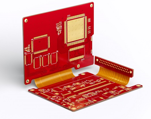
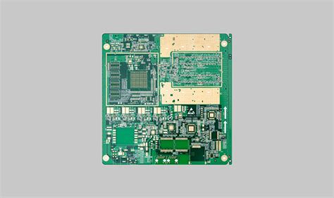
Rigid-Flex PCBs: Combining Flexibility And Rigidity For Optimal Performance
Rigid-flex PCBs, a hybrid of rigid and flexible circuit boards, offer a unique combination of flexibility and rigidity, making them an optimal choice for various advanced electronic applications. These innovative circuit boards are designed to integrate the best features of both rigid and flexible PCBs, thereby providing enhanced performance, reliability, and design versatility. As technology continues to evolve, the demand for more compact, efficient, and durable electronic devices has led to the increased adoption of rigid-flex PCBs across multiple industries.
One of the primary advantages of rigid-flex PCBs is their ability to maintain electrical connectivity while being subjected to mechanical stress.
This is particularly beneficial in applications where space constraints and dynamic movements are prevalent. For instance, in the aerospace and defense sectors, rigid-flex PCBs are utilized in avionics systems and military equipment, where they must endure extreme conditions and vibrations without compromising performance. Similarly, in the medical field, these PCBs are employed in devices such as pacemakers and hearing aids, where reliability and miniaturization are critical.
Moreover, rigid-flex PCBs offer significant design flexibility, allowing engineers to create more complex and compact electronic assemblies.
By combining rigid and flexible layers, these PCBs can be bent and folded to fit into tight spaces, reducing the overall size and weight of the final product. This is particularly advantageous in consumer electronics, where the demand for smaller, lighter, and more powerful devices continues to grow. Smartphones, tablets, and wearable technology are prime examples of products that benefit from the compact and efficient design enabled by rigid-flex PCBs.
In addition to their mechanical and design advantages, rigid-flex PCBs also provide improved signal integrity and reduced interconnection issues.
The seamless integration of rigid and flexible sections eliminates the need for connectors and cables, which are potential points of failure and sources of signal loss. This results in a more reliable and robust electronic system, with enhanced performance and longevity. Furthermore, the reduced number of interconnections simplifies the assembly process, leading to lower manufacturing costs and increased production efficiency.
Despite their numerous benefits, the design and manufacturing of rigid-flex PCBs present certain challenges.
The complexity of these hybrid boards requires advanced design tools and expertise to ensure optimal performance and reliability. Engineers must carefully consider factors such as material selection, layer stack-up, and thermal management to achieve the desired balance between flexibility and rigidity. Additionally, the manufacturing process for rigid-flex PCBs is more intricate than that of traditional rigid or flexible boards, necessitating specialized equipment and techniques.
Nevertheless, the advantages of rigid-flex PCBs far outweigh the challenges, making them an increasingly popular choice for a wide range of applications.
As technology continues to advance, the demand for more sophisticated and reliable electronic systems will drive further innovation in rigid-flex PCB design and manufacturing. By combining the best attributes of rigid and flexible circuit boards, rigid-flex PCBs offer a versatile and high-performance solution that meets the evolving needs of modern electronic devices.
In conclusion, rigid-flex PCBs represent a significant advancement in the field of electronic circuit design, providing a unique combination of flexibility and rigidity that enhances performance, reliability, and design versatility. Their ability to withstand mechanical stress, reduce interconnection issues, and enable compact designs makes them an ideal choice for various industries, including aerospace, medical, and consumer electronics. As the demand for more advanced and efficient electronic systems continues to grow, rigid-flex PCBs will undoubtedly play a crucial role in shaping the future of technology.