Flex rigid pcb design rules
Understanding The Basics Of Flex Rigid PCB Design Rules
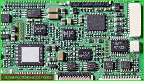
In the realm of modern electronics, the design of printed circuit boards (PCBs) plays a crucial role in the functionality and reliability of devices. Among the various types of PCBs, flex-rigid PCBs have gained significant attention due to their unique combination of flexibility and rigidity, which allows for innovative design solutions in compact and complex electronic devices. Understanding the basics of flex-rigid PCB design rules is essential for engineers and designers aiming to optimize the performance and durability of their products.
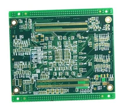
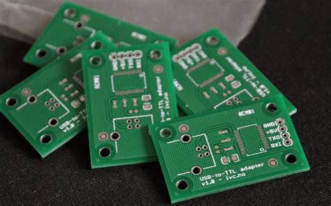
Flex-rigid PCBs are composed of both flexible and rigid substrates, seamlessly integrated to form a single circuit board.
This hybrid structure offers the advantage of reducing the number of connectors and interconnections required, thereby enhancing signal integrity and reducing the risk of connection failures. To achieve these benefits, it is imperative to adhere to specific design rules that govern the layout and fabrication of flex-rigid PCBs.
One of the fundamental considerations in flex-rigid PCB design is the selection of appropriate materials.
The flexible sections typically use polyimide films due to their excellent thermal stability and mechanical properties, while the rigid sections often employ FR-4 or similar materials. The choice of materials directly impacts the board’s performance, including its ability to withstand bending and thermal cycling. Therefore, designers must carefully evaluate the material properties to ensure compatibility with the intended application.
Transitioning from material selection to layout design, it is crucial to consider the bend radius in the flexible sections.
The bend radius is the minimum radius that the flexible part of the PCB can be bent without causing damage. Adhering to the recommended bend radius is vital to prevent stress fractures and maintain the integrity of the conductive traces. Typically, a larger bend radius is preferred to minimize stress, but this must be balanced with the space constraints of the device.
Moreover, the placement of components and traces requires meticulous attention.
In flex-rigid PCBs, it is advisable to avoid placing components or vias in the bend areas, as these can be susceptible to mechanical stress and potential failure. Instead, components should be strategically positioned in the rigid sections, where they are less likely to experience mechanical deformation. Additionally, trace routing should be optimized to minimize the number of bends and ensure smooth transitions between the flexible and rigid areas.
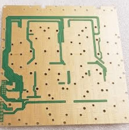
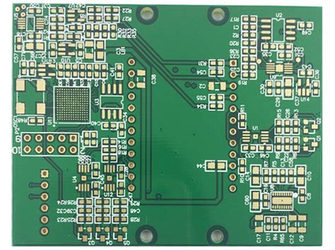
Another critical aspect of flex-rigid PCB design is the stack-up configuration.
The stack-up defines the arrangement of conductive and insulating layers within the PCB. A well-designed stack-up can significantly influence the board’s electrical performance, including impedance control and signal integrity. Designers must carefully plan the stack-up to accommodate the specific requirements of the application, considering factors such as layer count, thickness, and dielectric properties.
Furthermore, thermal management is a key consideration in flex-rigid PCB design.
The combination of flexible and rigid materials can lead to varying thermal expansion rates, potentially causing delamination or warping. To mitigate these risks, designers should incorporate thermal reliefs and consider the use of thermal vias to facilitate heat dissipation. Proper thermal management ensures the longevity and reliability of the PCB under varying operating conditions.
In conclusion, the design of flex-rigid PCBs involves a comprehensive understanding of material properties, layout considerations, stack-up configurations, and thermal management strategies. By adhering to established design rules, engineers can harness the advantages of flex-rigid PCBs, creating innovative solutions that meet the demands of modern electronic devices. As technology continues to evolve, mastering these design principles will be essential for staying at the forefront of PCB design and manufacturing.
Key Considerations For Flex Rigid PCB Stack-Up Design
In the realm of modern electronics, the design of flex-rigid printed circuit boards (PCBs) has become increasingly significant due to their ability to combine the benefits of both flexible and rigid substrates. These hybrid PCBs are particularly advantageous in applications where space constraints and complex geometries are prevalent, such as in aerospace, medical devices, and consumer electronics. However, designing an effective flex-rigid PCB stack-up requires careful consideration of several key factors to ensure optimal performance and reliability.
To begin with, understanding the material selection is crucial in the design of flex-rigid PCBs.
The choice of materials impacts not only the mechanical properties but also the electrical performance of the board. Typically, the rigid sections are composed of standard FR-4 material, while the flexible sections use polyimide due to its excellent flexibility and thermal stability. It is essential to ensure compatibility between these materials to prevent issues such as delamination or warping during the manufacturing process. Moreover, the thickness of the materials should be carefully selected to balance flexibility and rigidity, which is vital for maintaining the structural integrity of the board.
Transitioning from material selection to layer configuration, the stack-up design must be meticulously planned to accommodate the specific requirements of the application.
The number of layers in a flex-rigid PCB can vary significantly, and each layer must be strategically placed to optimize signal integrity and minimize electromagnetic interference (EMI). For instance, signal layers should be positioned adjacent to ground planes to provide effective shielding and reduce crosstalk. Additionally, the placement of power and ground layers should be considered to ensure efficient power distribution and minimize voltage drop across the board.
Furthermore, the design rules for trace routing in flex-rigid PCBs are more stringent compared to traditional rigid PCBs.
The traces in the flexible sections must be designed to withstand mechanical stress and bending without compromising electrical performance. To achieve this, it is advisable to use curved traces instead of sharp angles, as this reduces stress concentration points. Additionally, maintaining a consistent trace width and spacing is essential to prevent impedance mismatches and signal degradation. The use of teardrop pads at the transition points between flexible and rigid sections can also enhance mechanical stability and reduce the risk of trace breakage.
In addition to trace routing, the via design in flex-rigid PCBs requires special attention.
Vias are critical for establishing electrical connections between different layers, and their placement and size can significantly impact the board’s reliability. In flexible sections, it is recommended to use staggered or offset vias to distribute mechanical stress more evenly. Moreover, the use of blind or buried vias can help reduce the overall thickness of the board and improve flexibility.
Finally, thermal management is a vital consideration in flex-rigid PCB design.
The combination of different materials and the presence of both flexible and rigid sections can lead to uneven heat distribution, which may affect the board’s performance. Implementing thermal vias, heat sinks, and proper ventilation can help dissipate heat effectively and maintain the board’s operational stability.
In conclusion, designing a flex-rigid PCB stack-up involves a comprehensive understanding of material properties, layer configuration, trace routing, via design, and thermal management. By carefully considering these factors, engineers can create robust and reliable flex-rigid PCBs that meet the demanding requirements of modern electronic applications.
Best Practices For Trace Routing In Flex Rigid PCBs
In the realm of electronics, the design of flex rigid printed circuit boards (PCBs) presents unique challenges and opportunities. These hybrid boards, which combine flexible and rigid substrates, are increasingly popular due to their ability to accommodate complex geometries and reduce the overall size and weight of electronic devices. However, to fully leverage the advantages of flex rigid PCBs, it is crucial to adhere to best practices for trace routing, ensuring both functionality and reliability.
To begin with, understanding the distinct characteristics of flex and rigid sections is essential.
The flexible part of the PCB allows for bending and folding, which can be advantageous in compact designs. However, this flexibility also introduces potential stress points that can affect trace integrity. Therefore, when routing traces in the flexible sections, it is advisable to use curved traces instead of sharp angles. This approach helps distribute mechanical stress more evenly, reducing the risk of trace cracking or delamination over time.
Moreover, maintaining consistent trace width and spacing is vital in both the flexible and rigid sections.
Variations in trace width can lead to impedance mismatches, which may affect signal integrity. In the flexible sections, it is particularly important to avoid abrupt changes in trace width, as these can become focal points for mechanical stress. By ensuring uniformity, designers can enhance the durability and performance of the PCB.
Transitioning from the flexible to the rigid sections requires careful consideration.
It is recommended to stagger the transition points of traces, rather than aligning them in a straight line. This staggered approach minimizes stress concentration at the transition, thereby enhancing the mechanical reliability of the board. Additionally, incorporating teardrop patterns at the junctions where traces meet pads or vias can further alleviate stress and improve manufacturability.
Another critical aspect of trace routing in flex rigid PCBs is the management of differential pairs.
These pairs are often used for high-speed signal transmission and require precise control over trace length and spacing to maintain signal integrity. In the flexible sections, it is important to route differential pairs symmetrically and maintain consistent spacing to prevent skew and signal degradation. Furthermore, using ground planes or reference layers can help shield these pairs from electromagnetic interference, ensuring optimal performance.
Thermal management is another consideration that cannot be overlooked.
The flexible sections of a PCB typically have lower thermal conductivity than their rigid counterparts, which can lead to localized heating and potential failure. To mitigate this, designers should consider using wider traces for power and ground connections in the flexible areas, facilitating better heat dissipation. Additionally, strategically placing thermal vias can help transfer heat away from critical components, maintaining the overall thermal balance of the board.
Finally, collaboration with manufacturers during the design phase is crucial.
Manufacturers can provide valuable insights into material selection, layer stack-up, and fabrication processes that can influence trace routing decisions. By engaging with manufacturers early on, designers can ensure that their designs are not only theoretically sound but also practically feasible.
In conclusion, the design of flex rigid PCBs demands a meticulous approach to trace routing, balancing electrical performance with mechanical reliability.
By adhering to best practices such as using curved traces, maintaining consistent trace width, and managing differential pairs effectively, designers can create robust and efficient PCBs that meet the demands of modern electronic applications. Through careful planning and collaboration, the potential of flex rigid PCBs can be fully realized, paving the way for innovative and compact electronic solutions.
Material Selection Guidelines For Flex Rigid PCB Manufacturing
In the realm of electronics manufacturing, the design and production of flex-rigid printed circuit boards (PCBs) have become increasingly significant due to their ability to combine the benefits of both flexible and rigid circuits. These hybrid PCBs are particularly advantageous in applications where space constraints and mechanical flexibility are critical, such as in aerospace, medical devices, and consumer electronics. However, the successful manufacturing of flex-rigid PCBs hinges on meticulous material selection, which plays a pivotal role in ensuring the reliability and performance of the final product.
To begin with, understanding the distinct layers that constitute a flex-rigid PCB is essential.
Typically, these boards consist of multiple layers of flexible and rigid substrates laminated together. The flexible layers are often made from polyimide, a material known for its excellent thermal stability and flexibility. Polyimide’s ability to withstand high temperatures without deforming makes it an ideal choice for applications that require repeated bending or flexing. On the other hand, the rigid sections are usually composed of FR-4, a glass-reinforced epoxy laminate that provides structural support and rigidity. The combination of these materials allows for the integration of complex circuitry in a compact form factor.
Transitioning to the adhesive materials used in flex-rigid PCBs, it is crucial to select adhesives that can maintain strong bonds between the flexible and rigid layers while accommodating the mechanical stresses encountered during operation.
Acrylic and epoxy-based adhesives are commonly employed due to their robust bonding properties and thermal resistance. These adhesives must be carefully chosen to ensure compatibility with both the polyimide and FR-4 materials, as well as to withstand the thermal cycles experienced during the PCB’s lifecycle.
Moreover, the choice of copper foil is another critical consideration in flex-rigid PCB design.
The copper foil serves as the conductive layer, and its thickness and type can significantly impact the board’s electrical performance and flexibility. Rolled annealed copper is often preferred for the flexible sections due to its superior ductility, which allows it to bend without cracking. In contrast, electrodeposited copper may be used in the rigid sections where flexibility is less of a concern. The thickness of the copper foil must be carefully balanced to provide adequate current-carrying capacity while maintaining the desired level of flexibility.
In addition to these material considerations, the environmental conditions in which the flex-rigid PCB will operate must also be taken into account.
Factors such as temperature extremes, humidity, and exposure to chemicals can all influence material selection. For instance, in high-temperature environments, materials with higher glass transition temperatures (Tg) should be selected to prevent deformation or delamination. Similarly, in applications where moisture resistance is critical, materials with low water absorption rates are preferable.
In conclusion, the material selection process for flex-rigid PCB manufacturing is a complex but crucial aspect that directly impacts the performance and reliability of the final product.
By carefully considering the properties and compatibility of materials such as polyimide, FR-4, adhesives, and copper foil, manufacturers can design flex-rigid PCBs that meet the demanding requirements of modern electronic applications. As technology continues to advance, the importance of informed material selection in PCB design will only grow, underscoring the need for ongoing research and development in this field.