Flexible Circuit Board Design Techniques: A Comprehensive Guide
Introduction
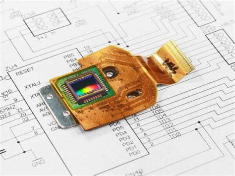
Flexible printed circuit boards (FPCBs) have become an essential component in modern electronics due to their lightweight, bendability, and ability to fit into compact spaces. Applications range from consumer electronics (smartphones, wearables) to medical devices, automotive systems, and aerospace technology. However, designing flexible circuits presents unique challenges compared to rigid PCBs. This article explores key design techniques for optimizing flexible circuit performance, reliability, and manufacturability.
1. Understanding Flexible Circuit Materials
1.1 Substrate Materials
The choice of substrate material significantly impacts flexibility, durability, and electrical performance. Common materials include:
- Polyimide (PI): High thermal stability, excellent flexibility, and chemical resistance. Ideal for dynamic flexing applications.
- Polyester (PET): Cost-effective but less durable than polyimide. Suitable for static applications.
- Liquid Crystal Polymer (LCP): High-frequency performance, low moisture absorption, but more expensive.
1.2 Conductive Materials
- Copper (Electrodeposited or Rolled-Annealed): Standard for flexible circuits. Rolled-annealed copper offers better flexibility.
- Silver or Carbon Ink: Used in printed electronics for low-cost, low-power applications.
1.3 Adhesives and Coverlays
- Acrylic or Epoxy Adhesives: Bond copper to the substrate.
- Coverlay (Polyimide with Adhesive): Protects traces instead of traditional solder mask.
2. Key Design Considerations for Flexible Circuits
2.1 Bend Radius and Flexibility Requirements
The bend radius is the minimum curvature a flex circuit can endure without damage. Key guidelines:
- Static Applications (One-time bend): Minimum bend radius ≥ 6x substrate thickness.
- Dynamic Applications (Repeated bending): Minimum bend radius ≥ 10x substrate thickness.
- Avoid Sharp Corners: Use gradual curves to reduce stress concentration.
2.2 Trace Routing and Layout Optimization
- Avoid 90° Angles: Use curved or 45° traces to minimize stress.
- Staggered Traces: In multilayer designs, offset traces to prevent overlapping stress points.
- Teardrop Pads: Strengthen connections between traces and pads to prevent cracking.
2.3 Layer Stackup and Multilayer Flex Design
- Single-Layer vs. Multilayer: Single-layer is simplest; multilayer provides higher density but reduced flexibility.
- Neutral Bend Axis: Place conductors near the center to balance tensile and compressive forces.
- Shielding: Use ground planes or conductive films to reduce EMI in high-speed designs.
2.4 Component Placement and Soldering
- Avoid Placing Components Near Bend Areas: Stress can crack solder joints.
- Use Flexible Soldermask Alternatives: Coverlay (polyimide film) is more durable than liquid photoimageable soldermask (LPSM).
- Stiffeners for Component Support: Add rigid sections (FR4, polyimide) under connectors or heavy components.
3. Signal Integrity and High-Speed Design
3.1 Impedance Control
- Microstrip vs. Stripline: Microstrip (surface traces) is easier to fabricate; stripline (embedded traces) offers better signal integrity.
- Controlled Dielectric Thickness: Ensure consistent spacing between signal and reference planes.
3.2 Crosstalk Mitigation
- Increase Spacing Between High-Speed Traces: Follow the 3W rule (spacing ≥ 3x trace width).
- Ground Shielding: Insert ground traces between high-speed signals.
3.3 High-Frequency Considerations
- Use Low-Dk Materials: LCP or specialized polyimides for RF/microwave applications.
- Minimize Discontinuities: Smooth transitions between rigid and flex sections.
4. Thermal Management
4.1 Heat Dissipation Techniques
- Thermal Vias: Transfer heat from components to external layers.
- Copper Thickness: Thicker copper improves heat spreading but reduces flexibility.
- Heat-Resistant Materials: Polyimide handles high temperatures better than PET.
4.2 Avoiding Thermal Stress
- Uniform Copper Distribution: Prevents warping during thermal cycling.
- Compatible CTE (Coefficient of Thermal Expansion): Match materials to minimize stress.
5. Manufacturing and Assembly Considerations
5.1 Design for Manufacturability (DFM)
- Panelization: Include fiducials and tooling holes for alignment.
- Tolerance for Laser Cutting vs. Punching: Laser cutting allows finer features but is slower.
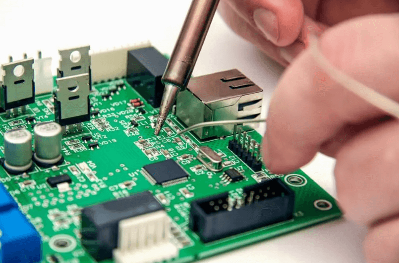
5.2 Handling and Testing
- Avoid Overhandling: Flex circuits are delicate; use proper fixtures.
- Automated Optical Inspection (AOI): Detects microfractures and misalignments.
- Bend Testing: Ensures reliability in dynamic applications.
6. Advanced Techniques for High-Reliability Flex Circuits
6.1 Rigid-Flex Designs
- Combines rigid and flexible sections for complex geometries.
- Transition Zones: Smoothly transition between rigid and flex areas to prevent cracking.
6.2 Stretchable Electronics (Emerging Tech)
- Uses serpentine traces or conductive elastomers for stretchable circuits.
- Applications in wearables and biomedical devices.
6.3 3D Printed Flexible Circuits
- Additive manufacturing enables rapid prototyping of custom flex circuits.
Conclusion
Designing flexible circuits requires a deep understanding of materials, mechanical stress, signal integrity, and manufacturability. By following best practices in bend radius optimization, trace routing, thermal management, and DFM, engineers can create reliable and high-performance flexible PCBs for cutting-edge applications. As technology evolves, innovations like stretchable electronics and 3D printing will further expand the possibilities of flexible circuit design.


