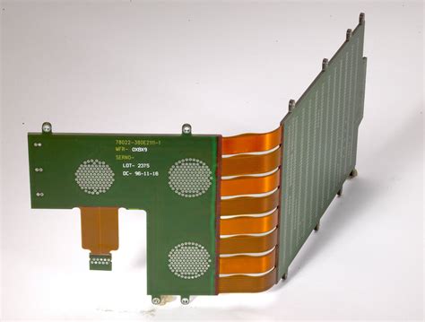
Flexible pcb button
Advantages Of Using Flexible PCB Buttons In Modern Electronics
Flexible PCB buttons have emerged as a pivotal component in the realm of modern electronics, offering a multitude of advantages that cater to the evolving demands of contemporary technology. As electronic devices become increasingly compact and sophisticated, the need for components that can adapt to these changes has never been more critical. Flexible PCB buttons, with their unique properties, provide a solution that addresses both the physical and functional requirements of modern electronic devices.
One of the primary advantages of flexible PCB buttons is their adaptability.
Unlike traditional rigid PCBs, flexible PCBs can be bent, folded, and twisted without compromising their functionality. This flexibility allows for more innovative and compact designs, enabling manufacturers to create devices that are not only smaller but also more ergonomic. For instance, in wearable technology, where space is at a premium, flexible PCB buttons can be integrated seamlessly into the design, providing functionality without adding bulk.
Moreover, the lightweight nature of flexible PCB buttons contributes significantly to the overall reduction in the weight of electronic devices.
This is particularly beneficial in applications such as aerospace and portable electronics, where every gram counts. By utilizing flexible PCBs, manufacturers can achieve the desired functionality while maintaining a lightweight profile, thus enhancing the user experience and broadening the scope of potential applications.
In addition to their physical advantages, flexible PCB buttons also offer enhanced durability.
The materials used in flexible PCBs are designed to withstand repeated bending and flexing, making them ideal for applications that require frequent movement or manipulation. This durability ensures a longer lifespan for the devices in which they are used, reducing the need for frequent repairs or replacements and thereby lowering the total cost of ownership.
Furthermore, flexible PCB buttons facilitate improved connectivity and signal integrity.
The ability to design circuits that can conform to various shapes and contours allows for more efficient routing of electrical signals. This can lead to reduced signal loss and interference, which is crucial in high-performance applications where precision and reliability are paramount. As a result, devices equipped with flexible PCB buttons can deliver superior performance compared to those using traditional rigid PCBs.
Another significant advantage of flexible PCB buttons is their potential for cost savings in the manufacturing process.
The integration of multiple components into a single flexible PCB can reduce the complexity of assembly, leading to lower labor costs and faster production times. Additionally, the reduction in the number of connectors and interconnects required can further decrease material costs and potential points of failure, enhancing the overall reliability of the device.
In conclusion, the advantages of using flexible PCB buttons in modern electronics are manifold. Their adaptability, lightweight nature, durability, improved connectivity, and potential for cost savings make them an attractive option for manufacturers looking to innovate and optimize their products. As technology continues to advance, the role of flexible PCB buttons is likely to become even more prominent, driving further developments in the design and functionality of electronic devices. By embracing these components, manufacturers can not only meet the current demands of the market but also anticipate and adapt to future trends, ensuring their products remain at the forefront of technological innovation.
Design Considerations For Flexible PCB Button Integration
When integrating flexible PCB buttons into electronic devices, several design considerations must be taken into account to ensure optimal functionality and reliability. Flexible printed circuit boards (PCBs) offer a unique advantage in electronic design due to their ability to conform to various shapes and spaces, making them ideal for applications where traditional rigid PCBs would be impractical. However, the integration of buttons on these flexible substrates requires careful planning and execution.
To begin with, material selection is a critical factor in the design of flexible PCB buttons.
The substrate material must be chosen based on its flexibility, durability, and compatibility with the intended application. Polyimide is a popular choice due to its excellent thermal stability and mechanical properties. Additionally, the conductive materials used for the button traces must be carefully selected to ensure reliable electrical performance. Copper is commonly used, but it may require additional surface treatments to enhance its adhesion and prevent oxidation.
Moreover, the layout of the flexible PCB must be meticulously designed to accommodate the button integration.
The placement of the buttons should be strategically planned to ensure ease of use and accessibility while maintaining the overall integrity of the circuit. It is essential to consider the bending and flexing of the PCB during operation, as excessive stress can lead to mechanical failure or compromised electrical connections. Therefore, incorporating strain relief features and optimizing the trace routing can significantly enhance the durability of the flexible PCB.
In addition to layout considerations, the method of button actuation plays a vital role in the design process.
Tactile feedback is often a desired feature in button design, providing users with a physical response when the button is pressed. This can be achieved through various mechanisms, such as dome switches or membrane overlays, each offering distinct advantages and challenges. The choice of actuation method should align with the device’s overall design goals, taking into account factors such as actuation force, travel distance, and tactile response.
Furthermore, environmental factors must be considered when designing flexible PCB buttons.
Devices that are exposed to harsh conditions, such as moisture, dust, or extreme temperatures, require additional protective measures to ensure long-term reliability. Conformal coatings or encapsulation techniques can be employed to shield the buttons and underlying circuitry from environmental stressors. These protective layers must be carefully selected to avoid interfering with the button’s functionality or the flexibility of the PCB.
Testing and validation are crucial steps in the design process to ensure that the flexible PCB buttons meet the desired performance criteria.
Rigorous testing under various conditions can help identify potential failure points and guide necessary design adjustments. This may include mechanical testing to assess the durability of the buttons under repeated use, as well as electrical testing to verify the integrity of the connections and signal transmission.
In conclusion, the integration of flexible PCB buttons into electronic devices requires a comprehensive approach that considers material selection, layout design, actuation methods, environmental protection, and thorough testing. By addressing these design considerations, engineers can successfully incorporate flexible PCB buttons into their products, leveraging the benefits of flexibility and space efficiency while ensuring reliable performance. As technology continues to advance, the demand for innovative and adaptable electronic solutions will drive further developments in flexible PCB design, opening new possibilities for device integration and functionality.
Manufacturing Process Of Flexible PCB Buttons: A Step-By-Step Guide
The manufacturing process of flexible PCB buttons is a meticulous and intricate procedure that requires precision and attention to detail. This process begins with the selection of appropriate materials, which is crucial for ensuring the durability and functionality of the final product. Typically, flexible PCBs are made from polyimide or polyester films due to their excellent flexibility and thermal stability. These materials are chosen for their ability to withstand the bending and flexing that flexible PCBs are often subjected to in various applications.
Once the material is selected, the next step involves designing the circuit layout.
This is a critical phase where engineers use specialized software to create a detailed blueprint of the circuit. The design must account for the specific requirements of the application, including the size, shape, and placement of the buttons. It is essential to ensure that the design is optimized for both performance and manufacturability, as any errors at this stage can lead to costly revisions later in the process.
Following the design phase, the circuit pattern is transferred onto the flexible substrate.
This is typically done using a process called photolithography, where a photoresist material is applied to the substrate and exposed to ultraviolet light through a mask that contains the circuit pattern. The exposed areas of the photoresist are then developed, revealing the underlying substrate, which is subsequently etched to create the circuit traces. This step requires precision to ensure that the circuit paths are accurately formed and free of defects.
After the circuit pattern is established, the next step is to apply a protective layer over the circuit.
This is often achieved by laminating a coverlay or solder mask onto the surface of the flexible PCB. The coverlay serves to protect the circuit from environmental factors such as moisture and dust, while also providing electrical insulation. It is important to ensure that the coverlay is properly aligned and adhered to the substrate to prevent any potential issues during the operation of the PCB.
The process then moves on to the assembly of the flexible PCB buttons.
This involves attaching the necessary components, such as conductive pads and domes, to the circuit. The conductive pads are typically made from materials like copper or silver, which provide excellent electrical conductivity. The domes, often made from metal or polyester, are placed over the conductive pads to create the tactile feedback that is characteristic of PCB buttons. This assembly process requires careful alignment and soldering to ensure that the buttons function correctly.
Finally, the completed flexible PCB buttons undergo rigorous testing to verify their performance and reliability.
This testing phase is crucial for identifying any defects or issues that may have arisen during the manufacturing process. Tests may include electrical conductivity checks, mechanical stress tests, and environmental simulations to ensure that the buttons can withstand the conditions they will encounter in their intended applications.
In conclusion, the manufacturing process of flexible PCB buttons is a complex and detailed procedure that involves multiple stages, from material selection and design to assembly and testing. Each step is critical to ensuring the quality and functionality of the final product, and requires a high level of expertise and precision. By following this step-by-step guide, manufacturers can produce flexible PCB buttons that meet the demanding requirements of modern electronic devices.
Applications Of Flexible PCB Buttons In Wearable Technology
Flexible PCB buttons have emerged as a pivotal component in the rapidly evolving field of wearable technology. As the demand for more compact, efficient, and versatile electronic devices continues to grow, the integration of flexible printed circuit boards (PCBs) into wearable technology has become increasingly prevalent. These flexible PCBs offer a myriad of advantages, including their lightweight nature, adaptability, and durability, making them ideal for use in a variety of wearable applications.
One of the primary applications of flexible PCB buttons in wearable technology is in the realm of fitness and health monitoring devices.
These devices, which include smartwatches, fitness trackers, and heart rate monitors, require components that can conform to the contours of the human body while maintaining functionality. Flexible PCB buttons are particularly well-suited for this purpose, as they can be seamlessly integrated into the design of these devices, allowing for a more comfortable and ergonomic user experience. Moreover, the flexibility of these PCBs ensures that the buttons can withstand the constant movement and stress associated with physical activity, thereby enhancing the durability and longevity of the devices.
In addition to fitness and health monitoring, flexible PCB buttons are also being utilized in the development of smart clothing.
This innovative application involves embedding electronic components into textiles to create garments that can perform a variety of functions, such as monitoring vital signs, providing haptic feedback, or even controlling other devices. The use of flexible PCBs in smart clothing is particularly advantageous due to their ability to bend and flex without compromising performance. This characteristic allows for the creation of garments that are not only functional but also comfortable and unobtrusive, thereby increasing their appeal to consumers.
Furthermore, flexible PCB buttons are playing a crucial role in the advancement of augmented reality (AR) and virtual reality (VR) wearables.
These devices, which often take the form of headsets or glasses, require intricate electronic components that can be integrated into compact and lightweight designs. Flexible PCBs offer a solution to this challenge by providing a means of incorporating buttons and other controls into the limited space available in these devices. This integration not only enhances the user experience by providing intuitive and accessible controls but also contributes to the overall aesthetic and functionality of the AR and VR wearables.
Moreover, the use of flexible PCB buttons extends to the realm of medical wearables, where they are employed in devices designed to monitor and manage various health conditions.
These devices, which include glucose monitors, ECG patches, and pain management systems, require components that can conform to the body and provide reliable performance over extended periods. Flexible PCBs are particularly well-suited for these applications, as they offer the necessary flexibility and durability to ensure consistent and accurate monitoring.
In conclusion, the applications of flexible PCB buttons in wearable technology are vast and varied, spanning from fitness and health monitoring devices to smart clothing, AR and VR wearables, and medical devices. Their unique properties, including flexibility, durability, and adaptability, make them an indispensable component in the design and development of modern wearable technology. As the industry continues to innovate and evolve, it is likely that the role of flexible PCB buttons will only continue to expand, further solidifying their importance in the future of wearable technology.