Four key points of esd protection circuit and pcb design
1.What is ESD?
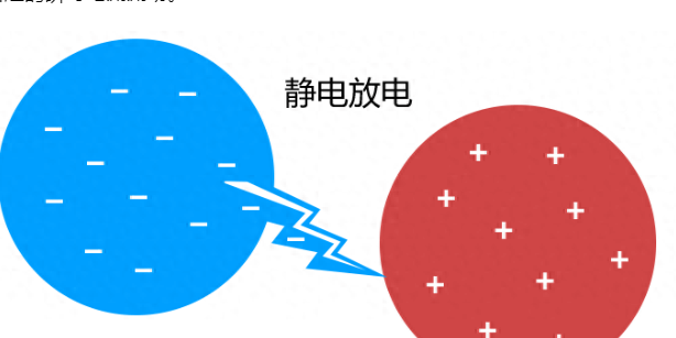
ESD stands for electrostatic discharge. Many materials can conduct electricity and accumulate charge. ESD occurs due to triboelectric charging (friction between materials) or electrostatic induction. Whenever this happens, an object develops a fixed charge (static electricity) on its surface. When this object is placed too close to another charged object or material, the voltage difference causes current to flow between them until the charge balance is restored.
Thus, electrostatic discharge can be defined as the instantaneous flow of current between two charged materials or objects caused by contact, short circuit, or dielectric breakdown.
For consumer products, ESD and dielectric breakdown in air usually occur when the electric field between two points is greater than 40 kV/cm. Factors such as air pressure, temperature, and humidity can affect the strength of the electric field. For example, high humidity in some environments can cause the air to be more conductive, which can dissipate some of the charge and increase the voltage required for ESD.
2.How does ESD affect PCBs?
Static electricity is common in life, but the voltage of static charge can reach several thousand volts, which can cause great harm to components.
When this voltage difference is large enough, there will be a conduction path for current, resulting in a huge current pulse. As the current pulse develops, high heat is dissipated within the components and conductors of the PCB itself. Under extreme field strengths and generated currents, the PCB may be damaged and components may be destroyed.
This heat dissipation is basically an IR drop, where the natural DC resistance of the components in the PCB produces a voltage drop and reaches high temperatures. ESD can occur in some common locations on the PCB, so ESD protection in the PCB should focus on certain specific areas. For example:
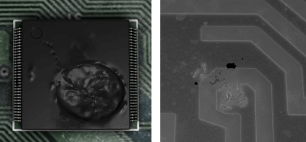
- ESD in integrated circuits
ESD pulses cause current to flow through the die on the integrated circuit, generating high heat that can damage components. An example of an integrated circuit package and the traces on the semiconductor chip are shown below.
Extreme ESD damage on an IC package (left) and die (right)
Especially now that many chips are manufactured using photolithographic features that cannot withstand high voltage drops, even DC values above the operating voltage may affect the chip.
- ESD in connectors
The connector itself is not an ESD source, but static charges accumulated on it can cause ESD. Someone plugging in a chip, unplugging a cable, or pressing a button can all cause static electricity to the device. Floating pins can generate ESD due to static charge transfer on floating conductors. Finally, when the connector is plugged into a socket, ESD may be generated, resulting in sparks.
Metal shields and floating pins on connectors are common locations for ESD events in some consumer and industrial products.
Metal shields and floating pins on connectors are common locations for ESD events in some consumer and industrial products
The simple solution to dealing with floating pins is to ground them. Shielded connectors should also have a grounded shield connected to the chassis and ultimately to earth. It should be a low impedance connection directly to the chassis, without providing this connection through capacitors, and without routing ESD current to ground through the PCB.
Almost every element of PCB design (traces, wiring, layers, electronic component placement and spacing) will affect the PCB ESD protection on the board. Therefore, ESD protection circuits must be considered early in the design.
III. ESD protection circuit design
- TVS diodes and diode circuits
TVS diode protection circuits are one of the most common circuits in non-industrial low-voltage settings. Compared with other ESD protection components embedded in power management ICs or microcontrollers, TVS surge diode protectors can provide higher voltage suppression, as shown in the example below.
The figure below is an example of an ESD protection circuit, which consists of parallel TVS diodes on differential I/O.
ESD protection circuit example
1) Typical voltage clamping diode circuit
The typical voltage clamping diode circuit is shown below. This voltage clamping circuit mainly limits the voltage accumulation at the input of the buffer.
Under normal conditions, diodes D1 and D2 are reverse biased, and diode D1 is forward biased and conducts whenever the voltage at the input is greater than the supply rail voltage. Similarly, when the input voltage is below ground, diode D2 is forward biased and conducts from ground to the input.
The figure below shows the Zener diode used in the ESD protection circuit on the single-ended buffer I/O.
Zener diode used in the ESD protection circuit on the single-ended buffer I/O.
The above circuit can use some simple diodes with high reverse bias breakdown voltage (such as Zener diodes), or TVS diodes combined in parallel or back-to-back configuration. The main factors used to determine which type of diode to use are the breakdown voltage and forward current.
TVS diodes are divided into two types, both types of TVS diodes act as an open circuit under normal operating conditions and act as a short circuit to ground when an ESD surge occurs.
2) Unidirectional transient suppression diodes
The unidirectional TVS surge diodes used for ESD protection are shown below. TVS diodes are not necessarily simple Zener diodes, but can also be components that are specifically marketed as TVS diodes, as shown in the figure below.
The figure below shows a unidirectional TVS suppression diode on the power rail of the protected component.
Unidirectional TVS suppression diode on the power rail of the protected component
During the positive cycle of the ESD, this diode becomes reverse biased and operates in avalanche mode, causing the ESD current to flow from the input to ground. During the negative cycle, this TVS diode becomes forward biased and conducts the ESD current.
How unidirectional TVS diodes protect circuits from ESD: by blocking or allowing the ESD current to flow, depending on its polarity.
3) Bidirectional transient suppression diodes
The figure below shows a typical use of bidirectional TVS surge diodes to protect ESD sensitive components. This is just a simple arrangement, and an additional resistor can be added if additional current limiting is required.
The figure below shows a bidirectional TVS suppression diode on the power rail of the protected component.
Bidirectional TVS suppression diode on the power rail of the protected component
During the positive cycle of a transient ESD, one of the two diodes is forward biased and the other is reverse biased, which means that one diode conducts due to its forward bias, while the other operates in avalanche mode. In this way, both diodes form a path from the ESD source to ground. During a negative ESD cycle, the diodes swap their modes, creating a path again and the circuit remains protected.
2.Use TISP4350 overvoltage protector instead of TVS diode
This circuit is designed for overvoltage on telecommunications lines. Compared to TVS diode arrays, TISP4 provides a certain degree of universal protection against ESD events and overvoltage events from other sources.
Use TISP4350 overvoltage protector instead of TVS diode
The choice of protection device depends on many factors. Different models and types are designed for different voltage ranges, operating voltages, event durations, response times, etc.
3.Other ESD suppressor components
In addition to the above, there are several other ESD suppressor components, such as multilayer varistors, gas discharge tubes, and polymer-based suppressors. ESD suppression components are used to reduce the ESD voltage below a specific limit, thereby protecting a circuit or component group.
The suppressor component or circuit is connected in parallel to the vulnerable line, keeping the low ESD voltage within a certain limit and shunting the main ESD current to ground. Generally, relevant circuit examples can be found on the datasheet.
4.Specific case: gas discharge tube + TVS diode
One strategy for handling high voltage is to use a gas discharge tube in parallel with a TVS diode and inductor. The inductor and TVS diode are like a low-pass RL circuit, providing additional filtering and slowing down the rise time of the ESD pulse.
The following circuit is basically a low-pass filter with a large time constant, so the circuit will allow the nominal DC voltage to pass while providing high impedance to the ESD current through the discharge tube. The fuse at the input provides additional protection against large ESD voltages.
The figure below shows an ESD protection circuit design using TVS diodes and gas discharge tubes.
ESD protection circuit design using TVS diodes and gas discharge tubes
IV. ESD protection in PCB layout
- Optimize the impedance around the TVS
All PCB components and traces have parasitic inductance. In a typical protection scheme, there are four: the inductance between the ESD source and the TVS array (L1 and L2), the inductance between the TVS and ground (L3), and the inductance between the TVS and the protected integrated circuit.
Only when L4 is greater than L1-3 can the ESD current be forced to ground.
Optimize the impedance around the TVS
The figure below shows the PCB layout of a project. As can be seen from the figure below, there is a USB port in this part of the PCB. To protect the FT231X UART (U1), we placed a USBLC6-4SC6 ESD suppressor (U2) in the path between it and the port.
PCB ESD protection layout
There are 2 points to note here:
The suppressor (U2) is placed close to the ESD source (USB port), and the inductor L4 becomes much larger than L1, which forces the ESD current to flow to the TVS.
The suppressor is placed directly on the path from the ESD source to the protected IC, completely removing L2.
- Limiting EMI from electrostatic discharge
ESD generates strong voltage pulses that can generate electromagnetic interference (EMI) to other nearby signal lines. The main source of radiation is between the ESD source and the suppressor, which acts as an antenna.
If possible, the suppressor area should be designed away from other circuits and unprotected traces, otherwise they will transmit ESD signals to other ICs. Even without considering the inductance of each line, the protected line and the adjacent unprotected line can act as capacitors, allowing voltage surges to pass between the two lines. The following figure illustrates how an ESD pulse couples to an unprotected line:
ESD couples to nearby traces because the two traces act like a capacitor
Another way to limit EMI is to use straight lines and short paths because corners radiate EMI. In this case, using straight lines is not possible. Instead, we used a 45° bend.
PCB ESD protection circuit layout
- Proper use of VIA
In a multi-layer PCB, vias can be used as parasitic inductors to reduce unnecessary traces. In the figure below, the ESD source and the protected IC are on the same layer, while the TVS is on another layer. Here, the VIA works as L2, causing the ESD current to be split between the TVS and the IC, so this layout must be avoided.
In this case, although the TVS is on its path, a portion of the ESD current will flow to the protected IC.
PCB worst layout
Ideally, the ESD source and TVS should be placed on the same layer, as shown in the figure below. In this way, the ESD current flows through the TVS protection pins before flowing to the protected circuit through the VIA. In this case, the TVS is directly on the path from the ESD source to the protected circuit.
Best PCB layout for ESD protection
In this particular PCB design, the ESD source (USB connector) has two traces on two different layers. However, it is impossible to put the ESD source and TVS on the same horizontal plane, so an acceptable layout is adopted.
An opposite situation can also be encountered here: the TVS and the protected IC are on the same layer, but the ESD source (the two traces from the USB) are on a different layer. Even so, this is also the correct way to design the VIA, because the TVS protection pin will receive the ESD current before it flows to the IC.
VIA layout for ESD protection
If the ideal layout cannot be achieved, an acceptable compromise is to force the ESD current to flow to the TVS in the following way: Although this routing is not perfect for ESD protection, it can be adopted if there is no other choice.
Compromise routing with VIAS
4.Placement of ESD suppressors
After selecting an ESD suppressor that is compatible with the electrical characteristics of the circuit, the next thing to consider is where to place it. The placement should be such that the IC receives the lowest possible voltage surge when an ESD occurs.
For medium frequency signals and typical ESD pulses, PCB traces act like inductors, meaning their impedance increases with frequency (ωL). The circuit with TVS diodes now looks like this:
The impact of line inductance on ESD
From the figure above, we can clearly see that when L2>>L1, the diode triggers quickly. This also means that most of the current will be directed away from the protected line, and L2 will also dissipate any ESD left on the protected line.
This means that we need to place the TVS diode as close as possible to where ESD may occur. The inductance of the ESD suppressor connected to the line or ground should be minimized. The energy of the ESD pulse decreases as the trace length increases, so the trace length between the ESD suppressor and the protected IC should be as long as possible.
5.Properly add vias between ESD source and suppressor
If there are vias between the ESD source and suppressor, the vias will also cause coupling to the unprotected line. Ideally, there should not be any vias between the ESD source and the suppressor because it will increase the length of the line, resulting in increased inductance on the line. This has two adverse effects:
It will increase the ESD pulse energy in the protected line
It will increase the signal generated by the unprotected line through EMI
If the engineer has no other choice but to add vias, then he must ensure that the protection line and the suppressor are on the same side of the PCB, and the source is connected to the protection line after the via (Case 1 in the figure below).
The worst case is that the source line and the protection line are on the same side, and the ESD suppressor is The ESD suppressor is on the other side, which must be avoided (Case 2 in the figure below). In this case, it is better to use another via to connect the protected line after the ESD suppressor instead of directly connecting the ESD source directly to the protected line (Case 3 in the figure below).
Earn money to add vias to reduce the impact of ESD on the protected line
6.Proper ground wiring
It has been explained in the above content that we need to reduce the trace inductance between the source and the TVS diode to move the voltage pulse away from the IC we need to protect, where we assume that the ESD suppressor has good grounding. But in fact, there may be some inductance between the ESD source TVS diode or between the TVS diode and the ground, as shown in the figure below:
The parasitic inductance on the suppressor can direct more ESD voltage back to the IC
We can reduce L3 by placing the TVS as close to the signal source as possible. To reduce L4, we use vias to connect the TVS ground pin directly to the ground plane. If a direct connection is not possible, use multiple vias in parallel on the trace leading to the ground plane.
This should make the drill diameter larger on each via and pad size to increase the surface area (to combat skin effect). The ground vias on the TVS suppressor should be filled with non-conductive material to maintain a large surface area.