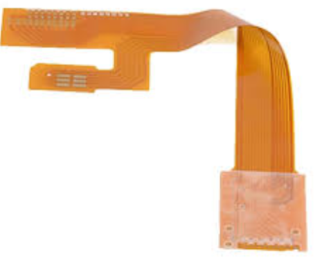
FPC opening – double sided FPC manufacturing process
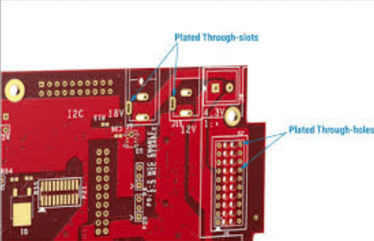
PCB board composition
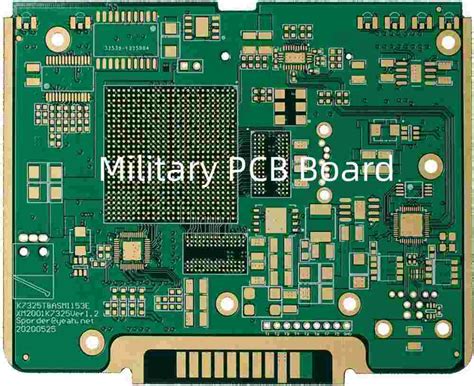
The current circuit board consists mainly of the following:
1. Line and Pattern: The line is used as the conduction between the originals. In the design, a large copper surface is additionally designed as the grounding and power layer. Lines and drawings are made at the same time.
2. Dielectric: used to maintain the insulation between the circuit and layers, commonly known as the substrate.
3. Through holes (or vias): Conductive vias allow two or more layers to conduct to each other. Larger vias are used for component insertion. Other non-via holes (nPTH) are commonly used as Surface mount positioning, fixing screws for assembly.
4. Solder resistant (Solder resistant / Solder Mask): Not all parts of the copper must be eaten on the tin part. Therefore, in the non-tiny area, a layer of material (usually epoxy resin) can be printed on the copper surface. Avoid short circuits between non-feeding tin lines. According to different processes, it is divided into green oil, red oil and blue oil.
5. Silk screen (Legend / Marking / Silk screen): This is an unnecessary structure, the main function is to mark the name and position box of each part on the circuit board to facilitate maintenance and identification after assembly.
6. Surface Finish: Since the copper surface is easily oxidized in the general environment and cannot be tin-plated (poor solderability), it will be protected on the copper surface where tin is to be eaten. The protection methods include HASL, ENIG, Immersion Silver, Immersion TIn, and OSP. Each method has advantages and disadvantages, which are collectively referred to as surface treatment.
PCB Features
1. Density-enhanced: For decades, the high density of PCBs has grown as integrated circuits have become more integrated and installation technology has advanced.
2. High reliability: A series of inspections, tests, and burn-in tests ensure that the PCB can work reliably for a long period of time (usually 20 years).
3. Designability: For various PCB performance (electrical, physical, chemical, mechanical, etc.) requirements, PCB design can be achieved through design standardization, standardization, etc., with short time and high efficiency.
4. Productivity: The use of modern management, can be standardized, scale (quantity), automation and other production, to ensure product quality consistency.
5. Testability: Established a relatively complete test method, test standards, a variety of test equipment and instruments to detect and identify the qualification and service life of PCB products.
Assemblability: PCB products are not only convenient for standard assembly of various components, but also can be automated, large-scale mass production. At the same time, PCBs and various component assembly parts can also be assembled to form larger parts and systems up to the complete machine.
6. Maintainability: Since PCB products and various component assembly parts are produced with standardized design and scale, these components are also standardized. Therefore, once the system fails, it can be quickly, easily, and flexibly replaced, quickly recovering the system. Of course, you can also give more examples. For example, the system is miniaturized, lightweight, and the signal transmission speed is increased.
Integrated circuit features
Integrated circuits have the advantages of small size, light weight, low lead-out and soldering points, long life, high reliability, and good performance. At the same time, the cost is low and it is convenient for large-scale production. It is not only widely used in industrial and commercial electronic equipment such as recorders, televisions, and computers, but also widely used in military, communications, and remote control. Assembling electronic devices with integrated circuits can increase the assembly density by several tens to several thousand times over that of transistors, and the stable operation time of the devices can also be greatly improved.
Integrated circuit application example
1. 555 touch timer switch
Integrated circuit IC1 is a 555 timing circuit, where it is connected to a monostable circuit. Normally there is no induced voltage at the P terminal of the touch panel. The capacitor C1 is discharged through the 7th pin of the 555. The output of the 3rd pin is low, the relay KS is released, and the light is off.
When it is necessary to turn on the light, touch the metal plate P by hand. The human body senses the clutter signal voltage from C2 to the trigger terminal of 555 so that the output of 555 goes from low to high, and the relay KS pulls in, the electric light spot. bright. At the same time, the interior of the 555 pin 7 is turned off, and the power supply charges C1 through R1. This is the start of timing.
When the voltage on the capacitor C1 rises to 2/3 of the power supply voltage, the 555 footpath 7 causes C1 to discharge, causing the output of the 3rd pin to change from a high level back to a low level, the relay releases, the light goes out, and the timing
The timing is determined by R1 and C1: T1=1. 1R1*C1. According to the value shown in the figure, the regular time is about 4 minutes. D1 can use 1N4148 or 1N4001.
2. Single power change dual power circuit
In the circuit of the drawing, the time base circuit 555 is connected to an astable circuit, and the 3-pin output frequency is 20 kHz and the duty ratio is 1:1 square wave. When the 3 pin is high, C4 is charged; when it is low, C3 is charged. Due to the existence of VD1 and VD2, C3 and C4 are charged only in the circuit without discharging. The maximum value of charge is EC, and the B terminal is grounded. At both ends of A and C, +/-EC dual power supply is obtained. The output current of this circuit exceeds 50mA.
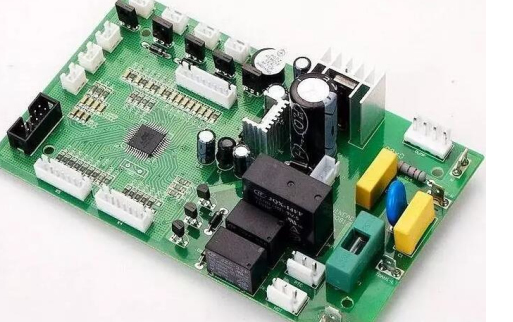
The difference between PCB board and integrated circuit
The integrated circuit generally refers to the integration of the chip, such as the North Bridge chip on the motherboard, and the inside of the CPU are all called integrated circuits, and the original name is also called an integrated block. Printed circuits refer to circuit boards that we usually see, and printed soldering chips on circuit boards.
The integrated circuit (IC) is soldered on the PCB board; the PCB board is the carrier of the integrated circuit (IC). The PCB board is a printed circuit board (PCB). Printed circuit boards appear in almost every type of electronic device. If there is an electronic component in a device, the printed circuit boards are mounted on PCBs of different sizes. In addition to fixing various small parts, the main function of the printed circuit board is to make electrical connections between the various parts on top of each other.
Simply put, an integrated circuit integrates a general-purpose circuit into a chip. It is a whole. Once it is damaged internally, the chip will be damaged, and the PCB can be soldered by itself, and the components can be replaced.