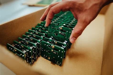
From schematic diagram to PCB design process, you must know
Six major PCB design skills, switching power supply design must be used!
In any switching power supply design, the physical design of the PCB board is the last link. If the design method is not appropriate, the PCB may radiate too much electromagnetic interference, causing unstable power supply operation. The following is an analysis of the matters that need to be paid attention to in each step.
1 From schematic diagram to PCB design process
Establish component parameters -> Input principle netlist -> Design parameter setting -> Manual layout -> Manual wiring -> Verify design -> Review -> CAM output.
2 Parameter setting
The spacing between adjacent wires must meet electrical safety requirements, and for ease of operation and production, the spacing should be as wide as possible. The minimum spacing must at least be suitable for the voltage to be tolerated. When the wiring density is low, the spacing between signal lines can be appropriately increased. The signal lines with a large difference in high and low levels should be as short as possible and the spacing should be increased. In general, the routing spacing is set to 8mil.
The distance from the edge of the inner hole of the pad to the edge of the printed circuit board should be greater than 1mm, so as to avoid pad defects during processing. When the trace connected to the pad is thin, the connection between the pad and the trace should be designed into a water drop shape. The advantage of this is that the pad is not easy to peel, but the trace and the pad are not easy to disconnect.
3 Component Layout
Practice has proved that even if the circuit schematic is designed correctly, improper design of the printed circuit board will have an adverse effect on the reliability of electronic equipment.
For example, if two thin parallel lines on the printed circuit board are close to each other, the signal waveform will be delayed and reflected noise will be formed at the terminal of the transmission line; interference caused by inconsiderate consideration of the power supply and ground wires will reduce the performance of the product. Therefore, when designing a printed circuit board, you should pay attention to using the correct method.
Each switching power supply has four current loops:
◆ Power switch AC loop
◆ Output rectifier AC loop
◆ Input signal source current loop
◆ Output load current loop Input loop
The input capacitor is charged by a current close to DC, and the filter capacitor mainly plays a broadband energy storage role; similarly, the output filter capacitor is also used to store high-frequency energy from the output rectifier and eliminate the DC energy of the output load loop.
Therefore, the terminals of the input and output filter capacitors are very important.
The input and output current loops should be connected to the power supply only from the terminals of the filter capacitors; if the connection between the input/output loop and the power switch/rectifier loop cannot be directly connected to the terminals of the capacitor, the AC energy will be radiated from the input or output filter capacitor to the environment.
The AC loop of the power switch and the AC loop of the rectifier contain high-amplitude trapezoidal currents, which have high harmonic components and frequencies much greater than the switching base frequency. The peak amplitude can be as high as 5 times the continuous input/output DC current amplitude, and the transition time is usually about 50ns.
These two loops are most likely to generate electromagnetic interference, so these AC loops must be laid out before other printed lines in the power supply. The three main components of each loop, filter capacitors, power switches or rectifiers, inductors or transformers, should be placed adjacent to each other, and the components should be positioned so that the current path between them is as short as possible.
The best way to establish a switching power supply layout is similar to its electrical design. The best design process is as follows:
- Place the transformer
- Design the power switch current loop
- Design the output rectifier current loop
- Connect to the control circuit of the AC power supply circuit
Design the input current source loop and input filter Design the output load loop and output filter According to the functional unit of the circuit, when laying out all the components of the circuit, the following principles must be met:
● First, consider the size of the PCB.
When the PCB size is too large, the printed lines are long, the impedance increases, the anti-noise ability decreases, and the cost increases; if it is too small, the heat dissipation is poor, and the adjacent lines are susceptible to interference. The best shape of the circuit board is a rectangle with a length-to-width ratio of 3:2 or 4:3. The components located at the edge of the circuit board are generally not less than 2mm away from the edge of the circuit board.
● When placing components, consider the future welding and do not place them too densely.
● Center the core components of each functional circuit and lay them out around them. Components should be arranged evenly, neatly and compactly on the PCB. The leads and connections between components should be minimized and shortened as much as possible. The decoupling capacitor should be as close to the VCC of the device as possible.
● For circuits working at high frequencies, the distribution parameters between components should be considered. In general, components should be arranged in parallel as much as possible in circuits. In this way, it is not only beautiful, but also easy to assemble and weld, and easy to mass produce.
● Arrange the positions of each functional circuit unit according to the process of the circuit, so that the layout is convenient for signal flow and the signal keeps the same direction as much as possible.
● The first principle of layout is to ensure the wiring pass rate. When moving the device, pay attention to the connection of the flying wire and put the devices with connection relationship together.
● Reduce the loop area as much as possible to suppress the radiation interference of the switching power supply.
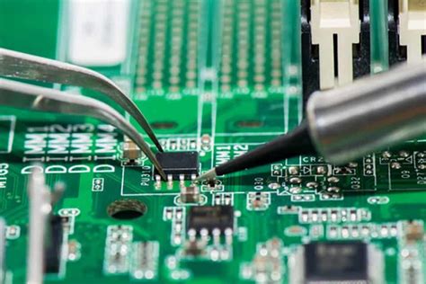
4 Wiring
The switching power supply contains high-frequency signals. Any printed line on the PCB can act as an antenna.
The length and width of the printed line will affect its impedance and inductance, thereby affecting the frequency response. Even the printed line passing the DC signal will couple to the RF signal from the adjacent printed line and cause circuit problems (even radiate interference signals again).
Therefore, all printed lines passing the AC current should be designed to be as short and wide as possible, which means that all components connected to the printed line and connected to other power lines must be placed very close.
The length of the printed line is proportional to the inductance and impedance it exhibits, while the width is inversely proportional to the inductance and impedance of the printed line. The length reflects the wavelength of the printed line response. The longer the length, the lower the frequency of the electromagnetic wave that the printed line can send and receive, and it can radiate more radio frequency energy.
According to the size of the printed circuit board current, try to increase the width of the power line and reduce the loop resistance.
At the same time, make the direction of the power line and the ground line consistent with the direction of the current, which helps to enhance the anti-noise ability.
Grounding is the bottom branch of the four current loops of the switching power supply. It plays a very important role as the common reference point of the circuit. It is an important method to control interference. Therefore, the placement of the grounding wire should be carefully considered in the layout. Mixing various groundings will cause unstable power supply operation.
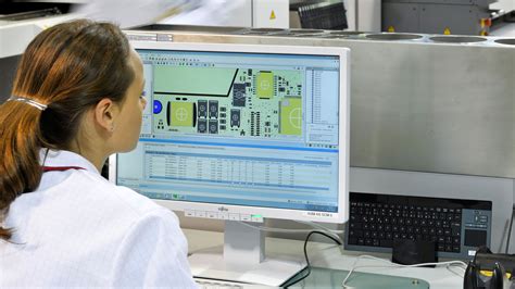
5 Inspection
After the wiring design is completed, it is necessary to carefully check whether the wiring design conforms to the rules set by the designer. At the same time, it is also necessary to confirm whether the rules set meet the requirements of the printed board production process. Generally, check whether the distance between the line and the line, the line and the component pad, the line and the through hole, the component pad and the through hole, and the through hole and the through hole is reasonable and meets the production requirements.
Whether the width of the power line and the ground line is appropriate, and whether there is still a place in the PCB that can widen the ground line.
Note: Some errors can be ignored. For example, part of the Outline of some connectors is placed outside the board frame, which will cause errors when checking the spacing. In addition, after each modification of the routing and vias, copper must be re-coated.
The review is based on the “PCB Checklist”, which includes design rules, layer definition, line width, spacing, pads, and via settings. It is also necessary to focus on reviewing the rationality of the device layout, the routing of the power and ground networks, the routing and shielding of the high-speed clock network, and the placement and connection of decoupling capacitors.
6 Design output
Notes on outputting photolithography files:
● The layers that need to be output are wiring layer (bottom layer), silk screen layer (including top silk screen and bottom silk screen), solder mask layer (bottom solder mask), drilling layer (bottom layer), and drilling file (NC Drill) must be generated
● When setting the silk screen layer layer, do not select Part Type, select the top (bottom) and silk screen layer Outline, Text, Line
● When setting each layer layer, select Board Outline, and when setting the silk screen layer layer, do not select Part Type, select the top (bottom) and silk screen layer Outline, Text