Function and method of PCB via plugging
Via hole, also known as conductive hole, plays the role of connecting circuits to each other. As electronic products develop towards “lighter, thinner, and smaller”, PCBs also develop towards high density and high difficulty. Therefore, a large number of SMT and BGA PCBs appear, and the plugging process is produced.
PCB plugging requirements
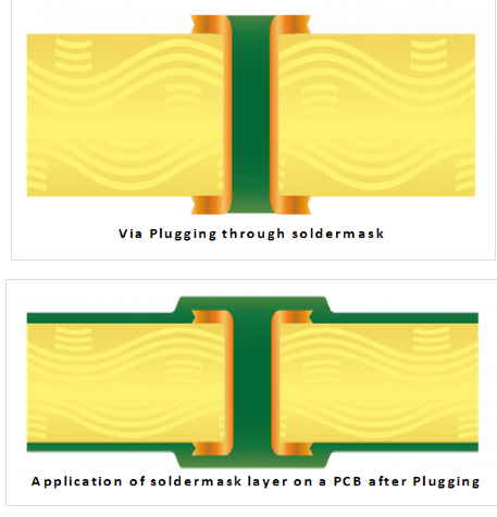
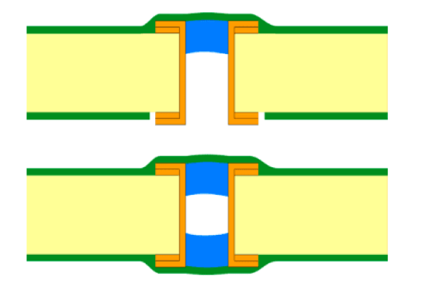
(i) There can be copper in the via hole, and solder mask can be plugged or not;
(ii) There must be tin-lead in the via hole, and there must be a certain thickness requirement (4 microns). Solder mask ink must not enter the hole, causing tin beads in the hole;
(iii) The via hole must be plugged with solder mask ink, opaque, and must not have tin rings, tin beads, and flatness.

Implementation of conductive hole plugging process
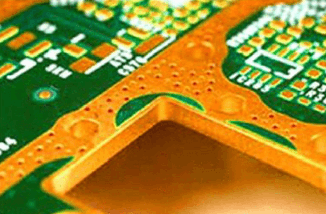
For surface mount boards, especially BGA and IC mounting, the via plugging requirements must be flat, with a convex and concave of plus or minus 1mil, and the via edge must not be red and tinned; the via hole must not have tin beads. In order to meet customer requirements, the via plugging process can be said to be varied, the process flow is particularly long, and the process control is difficult. There are often problems such as oil loss during hot air leveling and green oil solder resistance experiments; oil explosion after curing. Now, according to the actual production conditions, various PCB plugging processes are summarized, and some comparisons and explanations are made in the process and advantages and disadvantages:
Note: The working principle of hot air leveling is to use hot air to remove excess solder on the surface and holes of the printed circuit board, and the remaining solder is evenly covered on the pads, unblocked solder lines and surface packaging points. It is one of the surface treatment methods for printed circuit boards.
PCB via plugging function
- Avoid flux residue in the via hole;
- Prevent surface solder paste from flowing into the hole to cause cold soldering and affect mounting;
- Prevent tin beads from popping out during wave soldering and causing short circuit. Especially for BGA and IC mounting, the via plugging requirements are more stringent, requiring it to be flat, not red tinning, and no tin beads in the hole.
Common via plugging methods for PCB
- Ink plugging, using ink blocking net to complete the via plugging required by customers.
- Aluminum sheet plugging, drilling out the aluminum sheet to be plugged, making a screen to plug the hole.
- Resin plugging, using resin to plug the hole, this method is mainly used for a. Via plugging on multi-layer board BGA, using resin plugging can reduce the distance between holes and solve the problem of wires and wiring. b. Buried vias of inner layer HDI can balance the contradiction between the thickness control of the laminated dielectric layer and the design of the buried via filling glue of the inner layer HDI. C. Through holes with larger board thickness can improve product reliability.