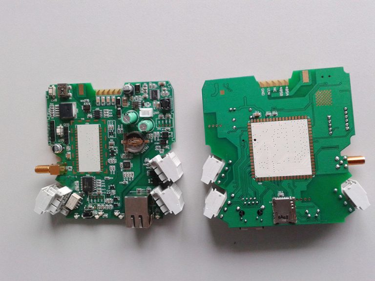
Grounding points for high-digital circuit PCBs
“Grounding” generally refers to connecting a circuit, device or system to a good conductor that serves as a reference potential point or reference potential surface, so as to establish a low-impedance channel between the circuit or system and the “ground”.
The ground wire is an equipotential body that serves as the potential reference point of the circuit or system. It is a common conductor for each circuit in the system. The current of any circuit will pass through the ground wire to form a loop.
However, any conductor has a certain impedance. When current passes through the ground wire, according to Ohm’s law, there will be voltage on the ground wire, so the ground wire is not an equipotential body.
Therefore, when designing a circuit or system, the assumption that the potential of each point on the ground wire must be equal is not valid. The actual situation is that there is a potential difference between each point on the bottom line, and some phase differences may be large.
The common impedance of the ground wire will cause a certain voltage to form between the grounding points, thereby generating grounding interference.
As mentioned above, the ground wire, as a conductor, has a certain impedance. As the name suggests, the impedance is composed of resistance and inductance, namely:
The impedance of the conductor is a function of the frequency. As the frequency increases, the impedance increases rapidly. For high-speed digital circuits, the clock frequency of the circuit is very high, and the pulse signal contains rich high-frequency components, so a large voltage will be generated on the ground wire, and the interference of the ground wire impedance on the digital circuit is considerable.
In the PCB design of electronic products, suppressing or preventing ground wire interference is one of the most important issues to consider. The so-called interference must occur between different unit circuits, components or systems, and ground wire interference refers to the signal interference generated by the common ground wire. Note that the signal mentioned here usually refers to AC signal or jump signal. There are many forms of ground wire interference. Some people classify it into two categories: ground wire loop interference and common impedance interference.
In fact, the electromagnetic coupling interference of the ground wire loop should also be added, so it is three categories.
- Ground loop interference. In the horizontal direction, the current on each wire is different, so a differential mode voltage will be generated, which will affect the circuit. Specifically, the ground wire current of “other circuit unit B” affects amplifiers A1 and A2 in the “ground wire loop” formed by J, N, L, and M. Since this interference is generated by the loop current formed by the cable and the ground wire, it is called ground loop interference.
- Ground loop electromagnetic coupling interference. On the PCB of the actual circuit, the “ground loop” formed by J, N, L, and M will surround a certain area. According to the law of electromagnetic induction, if there is a changing magnetic field in the area surrounded by this loop, an induced current will be generated in the loop, forming interference. The change of the magnetic field in space is everywhere, so the larger the area surrounded, the more serious the interference.
- Common impedance interference. Carefully examining the circuit structure shown in the figure above, we will find that one of J, N, L, and M is redundant. Removing any one of them can still meet the connectivity relationship of each grounding point and eliminate the ground loop. So, which connection is more reasonable to remove? At this time, we need to consider another type of interference problem-common impedance interference.
① Remove J: This is the worst solution. After J is removed, the ground loop seems to disappear, but another more terrible loop is formed (I, N, L, M), where I is the signal line, so the interference is more serious than when there is wire J.
②Remove M: The loop disappears, but we find that at this time, the ground current of amplifier A2 needs to flow through J and N to reach the ground zero point. Note that segment N is the common ground line of A1 and A2, so the voltage drop formed by the ground current of A2 on N is added to A1, forming interference. This interference caused by sharing a ground line is called “common impedance interference”.
③Remove L: Not only can the common impedance interference problem between A2 and A1 not be solved, but also the common impedance interference problem between “B unit circuit” and A1 and A2 is caused.
④Remove N: It seems that this is the last method. In fact, doing so will make M the “common impedance” of A1 and A2, which will also cause interference. There is still a problem! However, we noticed that the interference in this method is the interference of A1 to A2. A2 is the latter stage, and the working signal strength is much greater than A1. Therefore, the interference of A1 to A2 is unlikely to cause adverse consequences.
The most reasonable routing scheme is: remove N, and then connect the lower end of M directly to the “ground signal zero point”.
The above is about the causes of ground interference. The following are several common grounding methods. Combined with the previous understanding of the causes of ground interference, it will help us to correctly choose the grounding method with the least interference when actually designing PCB board circuits and design a reasonable circuit or system.
Signal grounding methods can be roughly divided into: single-point grounding, multi-point grounding, mixed grounding and floating grounding.
1.Single-point grounding.
Single-point grounding is to use a certain point in the entire circuit system as the reference point for grounding. All circuits and equipment ground wires must be connected to this point, and this point is used as the zero potential reference point of the circuit and equipment.
Single-point grounding is divided into series single-point grounding and parallel single-point grounding.
As shown in the figure below:
For the series single-point grounding method, if the power of the circuit is very large, a large circuit return current will be generated, and a voltage drop will be generated on the finite impedance. The difference in the voltage reference value between the circuit and the reference ground may cause the system to not work as expected.
If there are multiple circuits with different power levels, the series single-point grounding method cannot be used, because the high-power circuit generates a large return current, which will affect the low-power devices and circuits. If this grounding method must be adopted, then the most sensitive circuit must be set directly at the power input position and as far away from the low-power devices and circuits as possible. The series single-point grounding method and structure are relatively simple.
If the grounding leads of each circuit are relatively short, their impedance will also be relatively small. If the grounding levels of each circuit are not much different, this grounding method can be used.
In the parallel single-point grounding method, each circuit unit is connected to the same location with a separate ground wire. The advantage is that the location of each circuit is only related to the ground current and ground impedance of the circuit, and is not affected by other circuits. Low impedance interference between circuit units can be effectively avoided at low frequencies, but there are also many disadvantages.
Mainly manifested in:
First, each circuit uses an independent ground wire for grounding, which requires more ground wires, which will inevitably increase the length of the ground wire, thereby increasing the ground impedance, and the structure is complex and inconvenient to use;
secondly, this grounding method will cause coupling between the wires, and as the frequency increases, the ground wire impedance, ground wire inductance, and wire capacitance will increase. This grounding method is not suitable for high-frequency circuits.
Multi-point grounding.
Multi-point grounding means that each circuit and device that needs to be grounded in a system is directly connected to the ground plane closest to it, with the shortest grounding length on one side and the grounding impedance minimized.
When the operating frequency of the electronic system is higher than 1MHz, so that the operating wavelength is comparable to the length of the system ground lead, the ground wire is like a transmission line with a short-circuited terminal, and the current and voltage of the ground wire are distributed in a standing wave. The ground wire becomes a radiating antenna and cannot play the role of a ground wire.
In order to reduce the ground impedance and avoid radiation, the length of the ground wire should be less than 1/20 of the wavelength. Therefore, the single-point grounding method is unreasonable, and multi-point grounding technology is usually used. The multi-point grounding circuit has a simple structure, and the high-frequency standing wave phenomenon that may appear on the grounding line is significantly reduced, but multi-point grounding may cause many ground loops to form inside the device, which is easy to cause ground loop interference to sensitive parts inside the device.
Generally speaking, single-point grounding can be used when the frequency is below 1MHz, multi-point grounding can be used when the frequency is higher than 10MHz, and mixed grounding is usually used when the frequency is between 1 and 10MHz.
3.Mixed grounding.
Mixed grounding is a combination of single-point grounding and multi-point grounding.
This grounding method is often used when there are mixed high and low frequencies in the PCB.
two mixed grounding methods. For capacitive coupling circuits, a single-point grounding structure is presented at low frequencies, and a multi-point grounding state is presented at high frequencies. This is because the capacitor shunts the high-frequency current to the ground. The key to the success of this method is to understand the frequency used and the expected flow direction of the grounding current. Using capacitors and inductors in the grounding topology allows us to control the RF current in an optimized design. By determining the path that the RF current is to pass through, the wiring of the PCB can be controlled. Lack of understanding of the RF current loop may lead to radiation or sensitivity problems.
4.Floating ground.
Floating ground refers to the electrical insulation between the ground wire system of the equipment and the grounding system of the shell component to prevent the electromagnetic interference in the shell component from being transmitted to the equipment. However, since the equipment is not connected to the public ground, the floating ground is easy to cause static electricity accumulation between the two. When the charge accumulates to a certain extent, the potential difference between the equipment and the public ground may cause severe static electricity discharge and generate interference discharge current. Floating ground is not suitable for communication systems.
Knowing the above content, in the actual printing of BCB boards, the ground wire should be reasonably laid out based on the above theoretical basis. When laying out the ground wire, the following points should usually be noted:
- The digital ground and the analog ground should be separated;
- The ground wire of the digital circuit should not form a closed loop;
- In multi-layer PCBs, try to place the ground wire layer and the power layer in adjacent layers;
- The width design of the ground wire, power line and signal line should be reasonable.
The above points of attention should be studied and experienced slowly in actual operation.
When designing high-speed circuits, reasonable grounding design is the most effective electromagnetic compatibility design technology. According to statistics, 90% of electromagnetic compatibility problems are caused by improper wiring and grounding. Good wiring and grounding can not only improve immunity, but also reduce interference emission, and it is also possible to solve many electromagnetic interference problems at a low cost. Therefore, when designing PCB boards for high-speed circuits, reasonable grounding design is crucial.
It is generally recommended that power and signal currents should be returned through the “ground layer”, and this layer can also provide reference nodes for converters, reference voltage sources and other sub-circuits. However, even the widespread use of ground layers cannot guarantee that AC circuits have high-quality ground references.
shows a simple circuit made of a two-layer printed circuit board. There is an AC and DC current source on the top layer, one end of which is connected to via 1 and the other end is connected to via 2 through a U-shaped copper trace. Both vias pass through the circuit board and are connected to the ground layer. Ideally, the impedance is 0 and the voltage on the current source is 0 V.
Schematic and layout of a current source with a U-shaped trace on the PC board and a return through the ground plane.
This simple schematic is far from a true representation of the real situation, but understanding how current flows from via 1 to via 2 in the ground plane will help us see the real problem and find ways to eliminate ground noise in high-frequency layouts.
Inductance is proportional to the area of the current loop, and the relationship between the two can be explained by the right-hand rule and magnetic fields shown in Figure 2. Inside the loop, the magnetic fields generated by the current flowing along all parts of the loop reinforce each other. Outside the loop, the magnetic fields generated by different parts weaken each other. Therefore, the magnetic field is in principle confined to the loop. A larger loop has a higher inductance, which means that for a given current level, it stores more magnetic energy, has a higher impedance, and will therefore produce a larger voltage at a given frequency.
In the simple example shown in the figure, the loop with the smallest area is obviously the loop formed by the top trace of the U and the part of the ground plane directly below it. Figure 3 (left) shows that most AC current takes the path in the ground plane that encloses the smallest area, directly under the top conductor of the U. In practice, ground plane resistance causes low-IF current to flow somewhere between the direct return path and directly under the top conductor (right). However, even at frequencies as low as 1-2 MHz, the return path is close to under the top trace.
How to avoid layout problems? Once you understand the return path of current in the ground plane, you can identify and correct common layout problems. For example, in , path A is identified as the critical path and should be kept short, away from digital lines, and without vias. Path B is less important, but needs to pass through path A. This is usually done by cutting the ground plane under path A and routing path B through two vias and under path A.
Unfortunately, the result is that inductance is introduced into the ground return paths of both signals because the interrupted ground plane makes both loops larger. Path A carries a high-frequency signal, so an inductive voltage drop will appear across the opening in the ground plane. For a typical ECL or TTL signal, this voltage drop can be greater than hundreds of millivolts, enough to seriously affect the performance of a 12-bit, 10-MHz converter or an 8-bit, 20-MHz converter. A simple remedy is to add a conductor across the cut in the ground plane to keep the loop area small.
Power supply interference is another concern. The characteristic impedance of the power supply line must be as low as possible. To keep this ratio small, the ground plane needs to be always placed under the power supply line to reduce inductance and increase capacitance. Capacitance can be further increased by selectively placing bypass capacitors in strategic locations. If only capacitance is taken into account, for example, a 0.1 μF capacitor is placed on the power pin to reduce its impedance, then a power line with an inductance of 30 nH will have a damped oscillation of about 3MHz after each transient.