Guidelines for Drawing PCB Schematic
Schematic is the logical and visual representation of the circuit. It is the first step in designing an electronic product. Earlier, designers used to draw circuit diagrams on paper. Now, they have started using PCB design tools (M-CAD and E-CAD) that have simplified the design process. It is recommended that designers follow standard schematic guidelines to get a well-structured and error-free design.
Today, designers use numerous EDA (Electronic Design Automation) tools such as LCEDA, Altium, Allegro, Pads, Kicad, Tinycad, Express PCB, etc. These design tools ensure that the schematic circuit is error-free as they continuously monitor for logic and connection errors. Designers need to follow standard design rules to make the circuit machine-readable.
What is the Importance of Schematic?
Schematic is one of the important aspects of PCB design. A good schematic diagram shows a well-structured circuit diagram that clearly depicts the electrical connections between various electronic components. It should also be noted that a technically correct but crowded schematic is still a bad schematic as it can confuse the designer. A schematic can be a very valuable troubleshooting tool as it allows tracing the connections in the circuit.
Guidelines for Drawing PCB Schematics
To achieve a successful design, follow these standard schematic guidelines.
Page Size Selection
Most design tools offer different page sizes. Typically, these tools will choose a page size of A4. However, it should be noted that various other page sizes are also available. Designers should choose the size based on the size of their circuit design.
Page Naming Convention
The logical blocks of the schematic should be separated by pages. Pages can be named using letters A, B, C, etc. By doing this, we can place the pages in alphabetical order. An example of this naming convention is shown below.
A_Block Diagram
B_Power Supply
C_MCU Interface
D_Memory Interface
E_Revision History
Most designers often ignore the block diagram and revision history to save time. However, they are very helpful to other designers trying to understand the schematic. Most of the product based organizations make all such protocols and regulations mandatory.
Grid Setup
Though it is not a direct requirement of the designer, the tool needs to have some reference. Hence a grid system is followed. Having a grid helps the designer to reference the parts properly and make the connections. The circuit components and connections must always be on the grid which helps in probing the nets during analysis.
Page Title Block
The page title block appears in the footer of the schematic page. It is best to fill in all the required details like page size, update date, revision, document number, name/function of the circuit and company disclaimer. An example of a title block is shown below.
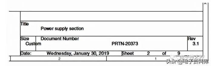
Page Title Block in Schematic
Comments/Comments
The designer needs to write necessary comments about the circuit. The comments can be written on a standalone document or on the schematic page. Usually, for complex designs, the comments are provided on a separate page. An example of comments could be jumper status, PCB layout constraints/guidelines, etc. A schematic with comments can be seen below.
Schematic with Annotations
Revision History
The revision history contains the changes made to the design. This document provides information including the date and description of the changes made, the names of the author and reviewers, and the review comments (if any). The revision history is usually placed on the first or last page of the schematic. An example of a schematic revision history is shown below.
Schematic Document Table of Contents
The table of contents lists the topics in the schematic document. Having this page helps the designer to easily find a specific module in a complex and large design. If the design is small and simple, this step can be skipped. An example of a ToC is given below.
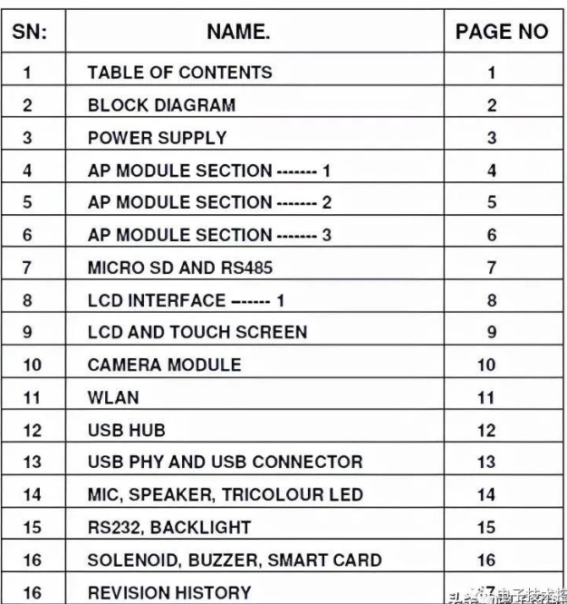
Table of Contents for a Schematic File
Block Diagram
A block diagram represents the different modules in the design and the signal flow. This greatly helps the reviewer understand the design for review. An example of a schematic block diagram can be seen below. Schematic Block Diagram High Speed PCB Design Guide 8 Chapters – 115 Pages – 150 Minutes to Read What’s Inside: Explanation of Signal Integrity Issues Understanding Transmission Lines and Controlled Impedance High Speed PCB Material Selection Process High Speed Layout Guide Download Now
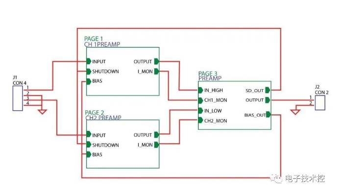
Hierarchical Schematic Design
If the design is complex and contains many modules, it is best to adopt a hierarchical design. The hierarchical schematic clearly shows the signal flow from one module to another as shown below. A detailed view of each module can be accessed by clicking on the corresponding module in the hierarchical schematic. Hierarchical Schematic Design
Component References
The following table shows the names of common electronic components and their corresponding reference designators used in any schematic. The designators are assigned according to IEEE standards. It is recommended to name components using their standard reference designators. Also, always use capital letters to designate schematic symbols.
Manufacturer Material Name Outgassing Data
Total Mass Loss % (1% max) Volatiles Collected %
(0.1% max)
Rogers RT/duroid 5870 0.02 <0.01
Rogers RT/duroid 5880 0.01 <0.01
Rogers RT/duroid 5880LZ 0.01 0.01
Rogers RT/duroid 6002 0.03 <0.01
Rogers RT/duroid 6006 0.01 <0.01
Nelco N4000-6 / 6FC 0.27 0.06
Nelco N4000-7 0.28 0
Nelco N4000-13 / 13SI 0.37 0.01
Nelco N4000-13EP/EPSI 0.14 0.01
Nelco N4000-29 0.10 0.01
Symbol Generation
Schematics consist of different types of components such as active components, passive components, and connectors. Active components include transistors, diodes, logic gates, processor ICs, FPGAs, op amps, etc. Components such as capacitors, inductors, and transformers are called passive devices. It is not recommended to create a new symbol unless the symbol for that component is not in the standard library. To learn more, check out How to Create Schematic and Symbol Libraries in KiCad.
Resistors
Resistors can be represented in two different ways, as shown below. Designers should take care to maintain consistency in the symbols used. Resistor Symbol The unit of resistance is Ohm, which is represented by the symbol “Ω”. Sometimes, the symbol “Ω” can be replaced with the letter “E”. Designers should ensure that consistent unit representation is followed throughout the design. All required data about the component should be entered in the design tool. This makes it easier to create a BOM (Bill of Materials) at the end of the design.
Polarized and non-polarized capacitors
Capacitors have two terminals, one positive and one negative. Care should be taken to mark the polarity of these terminals. Wrong polarity of capacitor terminals can lead to explosion. The following figure shows the capacitor symbol from the IEEE standard.
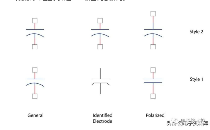
Polarized and non-polarized capacitors Designers should also ensure that the pin numbers assigned to the symbol should match the package layout exactly. Also, read about PCB manufacturing defects caused by land patterns.
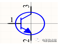
Transistors
A transistor is a three-terminal semiconductor device. The terminals are base, collector, and emitter. Designers should always refer to the component datasheet when mapping the pins in the package layout to the schematic symbol.
Transistor symbol with pin numbers When creating a symbol, it is important to enter a description of the component. This is useful for future reference or when a part becomes obsolete and needs to be replaced. Including these details in the BOM improves readability. The two images below show the full description field of a transistor symbol.
Transistor symbol description
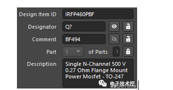
Component symbol description (Image credit: Altium)
Operational amplifier
It is important to create the symbol for the op amp according to the IEEE standard. Many designers often draw op amps based on their convenience, which often leads to a loss of readability. This can be caused by a lack of understanding and experience with CAD schematic tools.
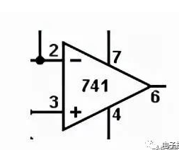
Operational Amplifier Symbol When creating a symbol, it is recommended to place all input pins on the left side and all output pins on the right side. Similarly, the power and ground pins can be placed on the top and bottom respectively. In the image shown, the input pins are 2 and 3, the output pin is 4, and the power and ground pins are 7 and 4 respectively. Designers should be careful while flipping or changing the symbol orientation. When we do this, there is a high chance that the positive and negative terminals will switch their positions. Therefore, care should be taken to cross-check each symbol with the manufacturer’s datasheet.
Heterogeneous Schematic Symbols
Complex devices such as FPGAs, memories, microprocessors, etc. are called heterogeneous components. These components have a large number of different types of pins such as data lines, input/output, address lines, control lines, and power lines. To maintain clarity and readability, designers should create multiple components of a single package such as UxA, UxB, UxC, and UxD. Given below is an example of such a heterogeneous schematic symbol for a component. Heterogeneous Schematic Symbols for Components
Power and Ground Symbols
The symbols for the power and ground pins are shown below.
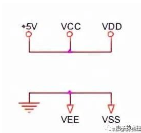
Power and Ground Symbols It is always a good idea to represent voltages with a “+” sign because negative voltages may be present on the board. Designers should follow standard and consistent conventions to represent voltage levels and their parts within the silicon. For example, +3.3V_IO, +3.3V_DG, +3.3V_AN +1.8V_Core, +1.2V_LVCore, +2.5_Vref, etc. Similarly, different types of grounds may be present on the board. The symbols are shown below.
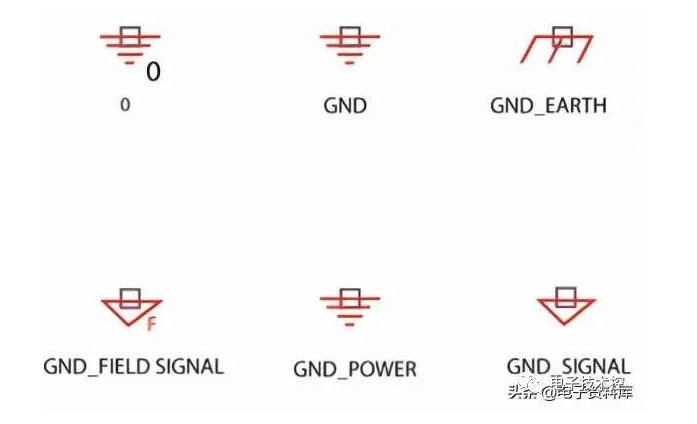
Different Types of Ground Symbols
Net Connections
Whenever you have two wires that form a junction and share an electrical connection, that junction needs to have a connection point. This is a standard practice in every schematic design.
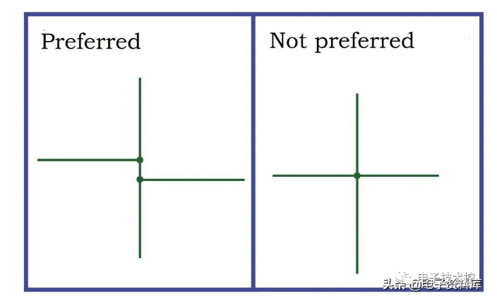
Net Connections in Schematic Design
Net Labeling Conventions
The purpose of a schematic is to make it easier for designers to understand your circuit. Unnecessary net connections should be minimized. This is commonly observed when the symbol of an integrated circuit (IC) is drawn on a schematic. Instead of drawing dozens of nets everywhere, the designer represents a net name for a specific pin, which is associated with a pin on another device. These pins will have the same name. Pins with the same name are assumed to be connected. This improves the readability of the schematic. The following image shows a series of named nets.
Off-page connections
Net labeling guidelines
Net naming is not required when the net is directly connected to another IC on the same page. However, if you want to connect the net to an IC on another page, then you need to name it. Designers can follow these simple rules when naming nets:
Signal names should always be written in uppercase and should be placed just above the net.
Avoid using long names. Preferably, names can have up to 4 letters.
Use an upper bar to describe active low or high signals. Pins with an upper bar are considered active low pins.
Open nets/connections should be removed.
Off-page connections
To improve readability, designers usually name nets in the schematic. This works fine when signals are to be connected on the same page. If you need to connect a net to a pin on a different page, then an off-page connector symbol should be used.
Signal flow representation
On a schematic page, signals flow from the left side of the page to the right side. Any power and ground connections are shown at the top or bottom of the page. Designers are advised to keep this in mind and keep the components accordingly.
Component Placement
Component placement in the schematic is one of the important tasks. This is because the layout engineer will keep the components accordingly. The parallel connection of capacitors is shown in the left figure. As we can see, the readability of the schematic is not up to par. Parallel connection of capacitors in schematic To improve readability, the connections can be made as shown below. Preferred parallel connection of capacitors in schematic Also read how to place components in KiCad.
Crystal Placement
The crystal placement in the schematic is always as shown below. The components connected to the crystal are always placed near it as the signals can be high frequency. Crystal Placement in Schematic
DRC Checking
Design Rule Checking (DRC) is a smart feature provided by CAD software to check the logical and physical integrity of the design. The checking is done for all enabled design rules and can be done online while you are designing.
Netlist Verification
When the schematic design is complete and ready to be imported into the layout, a netlist is generated. Netlist files can have two different extensions (.mnl and .txt). .mnl files are machine readable. .txt files show all the connections/nets between component pins. Manual verification of nets is recommended to avoid design errors. Also read about Gerber, ODB++ and other PCB design files required by manufacturers.
Bill of Materials (BOM)
Currently, CAD tools offer a key feature called BOM creation. Only designers can When creating or importing a component from a library, all the inputs are provided in the tool to generate a complete and adequate BOM. The inputs to the BOM can be MPN (Manufacturing Part Number), Footprint, Vendor Name, Vendor Part Number, etc. It is recommended to provide all the required information during symbol creation.
Schematic Checklist
The schematic checklist is the most commonly overlooked point in schematic creation. This is more about the process of organization, which is set based on past design experience. Having a checklist can avoid mistakes in the schematic and make the design more robust. Here is the checklist.
The pin numbers and labels of each component should be verified in relation to the datasheet.
Polarity checks should be done on all polarized components.
Check for overlapping labels and pin numbers.
Verify the base, collector and emitter pins of all transistors with the datasheet, schematic symbol and package footprint.
Verify the value, reference designator and location of the component.
Make sure the schematic symbol description is present. (MPN, Vendor Name, Vendor Part Number, etc.).
Check off-page connectors.
Look for inter-sheet references.
Decoupling capacitors check all ICs, ground pin separation based on signal type (analog, digital, signal, ground).
BOM checks quantities and part numbers.
When designers draw circuits in CAD tools, they should be aware that the schematic design is the input for the layout designer. The layout designer wants the schematic to be error-free so that the layout is well constructed and accurate.


