H bridge pcb
Designing an Efficient H Bridge PCB for Motor Control Applications
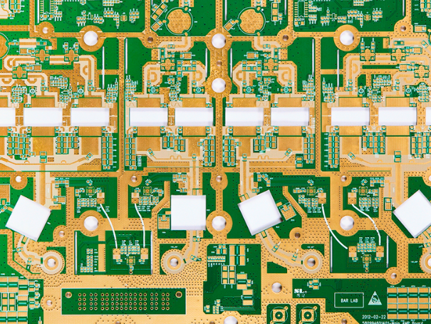
Designing an efficient H Bridge PCB for motor control applications is a critical task that requires a comprehensive understanding of both electronic components and circuit design principles. The H Bridge circuit is a fundamental building block in motor control systems, allowing for the control of the direction and speed of a motor. This is achieved by reversing the polarity of the motor’s voltage supply, which is facilitated by the H Bridge configuration. As such, the design of the PCB must be meticulously planned to ensure optimal performance and reliability.
To begin with, selecting the appropriate components is paramount.
The transistors or MOSFETs used in the H Bridge must be capable of handling the current and voltage requirements of the motor. It is essential to choose components with adequate ratings to prevent overheating and ensure longevity. Additionally, incorporating flyback diodes is crucial to protect the transistors from voltage spikes caused by the inductive load of the motor. These diodes provide a path for the back EMF generated when the motor is turned off, thereby safeguarding the circuit.
Once the components are selected, the layout of the PCB becomes the next focal point.
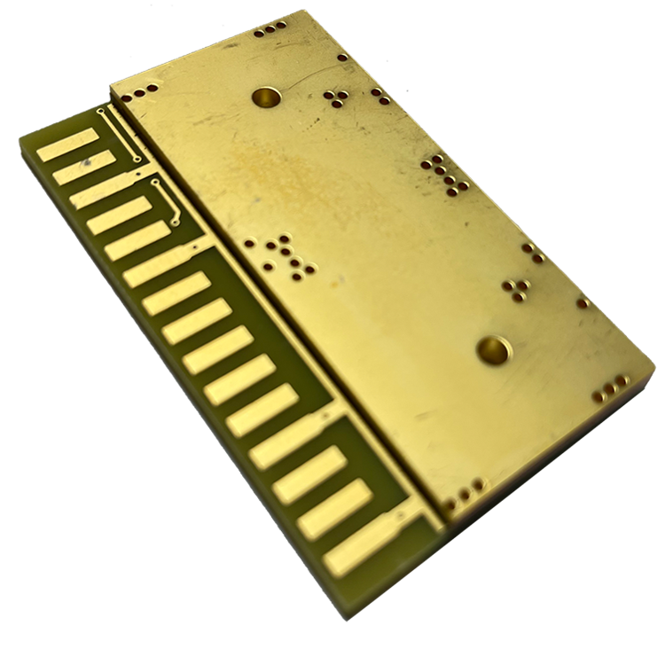
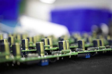
A well-designed layout minimizes parasitic inductance and resistance, which can lead to inefficiencies and potential circuit failures. Placing the transistors symmetrically and as close to the motor terminals as possible can help reduce these parasitic effects. Furthermore, ensuring that the traces carrying high current are wide enough to handle the load without excessive heating is vital. The use of copper pours for power and ground planes can also aid in reducing resistance and improving thermal management.
In addition to the physical layout, the routing of the PCB traces must be carefully considered.
It is advisable to keep the control signals separate from the power traces to minimize electromagnetic interference (EMI). This separation can be achieved by routing control signals on one layer of the PCB and power traces on another, using vias to connect them where necessary. Moreover, incorporating decoupling capacitors near the power pins of the transistors can help stabilize the voltage supply and reduce noise.
Thermal management is another critical aspect of designing an efficient H Bridge PCB.
The heat generated by the transistors during operation can lead to performance degradation and potential failure if not properly managed. Utilizing heat sinks or thermal vias can help dissipate heat away from the components. Additionally, selecting a PCB material with good thermal conductivity can further enhance heat dissipation.
Testing and validation are the final steps in the design process.
It is essential to thoroughly test the PCB under various load conditions to ensure it meets the desired performance criteria. This includes verifying the switching speed, checking for any signs of overheating, and ensuring that the motor operates smoothly in both forward and reverse directions.
In conclusion, designing an efficient H Bridge PCB for motor control applications involves a careful balance of component selection, layout design, trace routing, and thermal management. By paying close attention to these factors, one can create a robust and reliable PCB that meets the demands of modern motor control systems. Through meticulous planning and testing, the resulting design can provide efficient and precise control over motor operations, thereby enhancing the overall performance of the application.
Key Considerations for H Bridge PCB Layout and Design
When designing an H bridge PCB, several key considerations must be taken into account to ensure optimal performance and reliability. The H bridge circuit, commonly used for controlling the direction and speed of DC motors, requires careful attention to layout and design to minimize issues such as electromagnetic interference, heat dissipation, and signal integrity. By understanding these considerations, designers can create efficient and robust H bridge PCBs.
To begin with, component placement is a critical aspect of H bridge PCB design.
Proper placement can significantly reduce parasitic inductance and resistance, which are crucial for minimizing power losses and enhancing the overall efficiency of the circuit. It is advisable to place power components, such as MOSFETs or IGBTs, as close to each other as possible. This minimizes the loop area, thereby reducing the inductive effects that can lead to voltage spikes during switching events. Additionally, placing decoupling capacitors near the power supply pins of these components can help stabilize the voltage levels and reduce noise.
Transitioning to the topic of trace routing, it is essential to consider the current-carrying capacity of the traces.
The traces should be wide enough to handle the maximum current without excessive heating, which could lead to reliability issues or even failure. Utilizing thicker copper layers can also aid in managing higher currents. Furthermore, keeping the traces as short and direct as possible helps in reducing resistance and inductance, which are vital for maintaining signal integrity and reducing electromagnetic interference.
Another important consideration is the thermal management of the H bridge PCB.
Power components in the H bridge can generate significant heat, especially during high-current operations. Therefore, incorporating adequate thermal vias and heat sinks is crucial for dissipating heat effectively. Placing thermal vias under power components can facilitate heat transfer to other layers of the PCB, while heat sinks can be used to dissipate heat into the surrounding environment. Additionally, using thermal simulation tools during the design phase can help identify potential hotspots and optimize the thermal performance of the PCB.
Moreover, grounding is a fundamental aspect that cannot be overlooked.
A solid ground plane is essential for providing a low-impedance path for return currents, which helps in reducing electromagnetic interference and improving signal integrity. It is advisable to use a continuous ground plane and avoid splitting it with signal traces, as this can create ground loops and increase susceptibility to noise. Connecting the ground plane to the chassis ground at a single point can further enhance the noise immunity of the circuit.
In addition to these technical considerations, it is also important to adhere to industry standards and guidelines during the design process.
Standards such as IPC-2221 for general PCB design and IPC-9592 for power conversion devices provide valuable insights into best practices and can help ensure compliance with safety and performance requirements.
In conclusion, designing an H bridge PCB involves a careful balance of component placement, trace routing, thermal management, and grounding. By paying close attention to these key considerations, designers can create efficient, reliable, and high-performance H bridge circuits. As technology continues to advance, staying informed about the latest design techniques and tools will be essential for meeting the evolving demands of modern electronic applications.

Troubleshooting Common Issues in H Bridge PCB Circuits
When working with H Bridge PCB circuits, engineers and hobbyists alike often encounter a range of issues that can impede the functionality of their projects. Understanding these common problems and their solutions is crucial for ensuring the efficient operation of these circuits. An H Bridge is a type of electronic circuit that allows a voltage to be applied across a load in either direction, making it an essential component in controlling motors. However, like any complex electronic system, it is susceptible to various issues that can arise during design, assembly, or operation.
One of the most prevalent issues in H Bridge PCB circuits is overheating.
This can occur due to several factors, including excessive current flow, inadequate heat dissipation, or poor component selection. To mitigate overheating, it is essential to ensure that the components used are rated for the expected current levels. Additionally, incorporating heat sinks or fans can help dissipate heat more effectively. Proper PCB layout is also critical; ensuring that there is adequate spacing between components and using wider traces for high-current paths can significantly reduce the risk of overheating.
Another common problem is electromagnetic interference (EMI), which can disrupt the normal operation of the circuit.
EMI can be caused by poor grounding, inadequate shielding, or improper placement of components. To address this, it is advisable to use a ground plane in the PCB design, which can help minimize interference. Additionally, placing decoupling capacitors close to the power pins of integrated circuits can further reduce EMI. Shielding sensitive components and using twisted pair cables for connections can also be effective strategies in minimizing interference.
Short circuits are another issue that can plague H Bridge PCB circuits.
These can result from solder bridges, damaged components, or incorrect wiring. To prevent short circuits, it is crucial to inspect the PCB thoroughly after assembly, looking for any unintended connections or solder bridges. Using a multimeter to check for continuity can help identify potential short circuits before powering the circuit. Furthermore, ensuring that all components are correctly oriented and that connections are made according to the schematic can prevent wiring errors that lead to shorts.
In addition to these issues, incorrect component values can lead to suboptimal performance or even failure of the H Bridge circuit.
This can occur if resistors, capacitors, or other components are not selected according to the design specifications. Double-checking the component values against the schematic before assembly can prevent this issue. Additionally, simulating the circuit using software tools before building it can help identify potential problems with component values.
Finally, one must consider the possibility of software-related issues, especially in circuits that are controlled by microcontrollers or other programmable devices.
Bugs in the code can lead to erratic behavior or failure of the H Bridge circuit. To troubleshoot software issues, it is important to thoroughly test the code in a controlled environment, using debugging tools to step through the program and identify any logical errors.
In conclusion, while H Bridge PCB circuits are invaluable in controlling motor direction and speed, they are not without their challenges. By understanding and addressing common issues such as overheating, EMI, short circuits, incorrect component values, and software bugs, one can ensure the reliable operation of these circuits. Through careful design, assembly, and testing, these problems can be mitigated, leading to successful implementation in a variety of applications.
Optimizing Thermal Management in H Bridge PCB Designs
In the realm of electronic circuit design, the H bridge configuration is a fundamental component used to control the direction and speed of motors. As these circuits are integral to a wide range of applications, from robotics to automotive systems, optimizing their performance is crucial. One of the most significant challenges in H bridge PCB (Printed Circuit Board) designs is managing thermal performance. Effective thermal management is essential to ensure reliability, efficiency, and longevity of the circuit, as excessive heat can lead to component failure and reduced performance.
To begin with, understanding the sources of heat generation in an H bridge circuit is vital.
Typically, heat is produced by the power transistors, which are responsible for switching the current flow through the motor. These transistors, often MOSFETs or IGBTs, can generate substantial heat during operation, especially when handling high currents. Therefore, selecting components with low on-resistance and high thermal efficiency is a primary consideration. Additionally, the switching frequency and duty cycle of the transistors can influence heat generation, necessitating careful design choices to minimize thermal stress.
Transitioning to the PCB design itself, the layout plays a pivotal role in thermal management.
A well-designed PCB can effectively dissipate heat away from critical components. One strategy is to use wider and thicker copper traces, which can carry more current and distribute heat more evenly. Moreover, incorporating thermal vias—small holes filled with conductive material—can facilitate heat transfer from the top layer of the PCB to the bottom layer or to an internal ground plane, thereby enhancing thermal dissipation.
Furthermore, the use of heat sinks and thermal pads can significantly improve heat management.
Heat sinks, attached to the power transistors, increase the surface area available for heat dissipation, allowing for more efficient cooling. Thermal pads, on the other hand, provide a conductive path for heat to move from the component to the heat sink or PCB, reducing thermal resistance. These components should be carefully selected and positioned to maximize their effectiveness.
In addition to these hardware solutions, thermal simulation software can be an invaluable tool in the design process.
By simulating the thermal behavior of the H bridge circuit under various operating conditions, designers can identify potential hotspots and evaluate the effectiveness of different thermal management strategies. This proactive approach allows for optimization before physical prototypes are built, saving time and resources.
Moreover, considering the ambient environment in which the H bridge will operate is crucial.
Factors such as airflow, ambient temperature, and enclosure design can all impact thermal performance. For instance, ensuring adequate ventilation or incorporating active cooling methods, such as fans, can help maintain optimal operating temperatures.
In conclusion, optimizing thermal management in H bridge PCB designs is a multifaceted challenge that requires careful consideration of component selection, PCB layout, and environmental factors. By employing a combination of design strategies and simulation tools, engineers can enhance the thermal performance of their circuits, ensuring reliability and efficiency. As technology continues to advance, the importance of effective thermal management in electronic design will only grow, underscoring the need for ongoing innovation and attention to detail in this critical area.